Icosahedron LED Lamp Challenge

Project update:

Been working on the PCB designs.
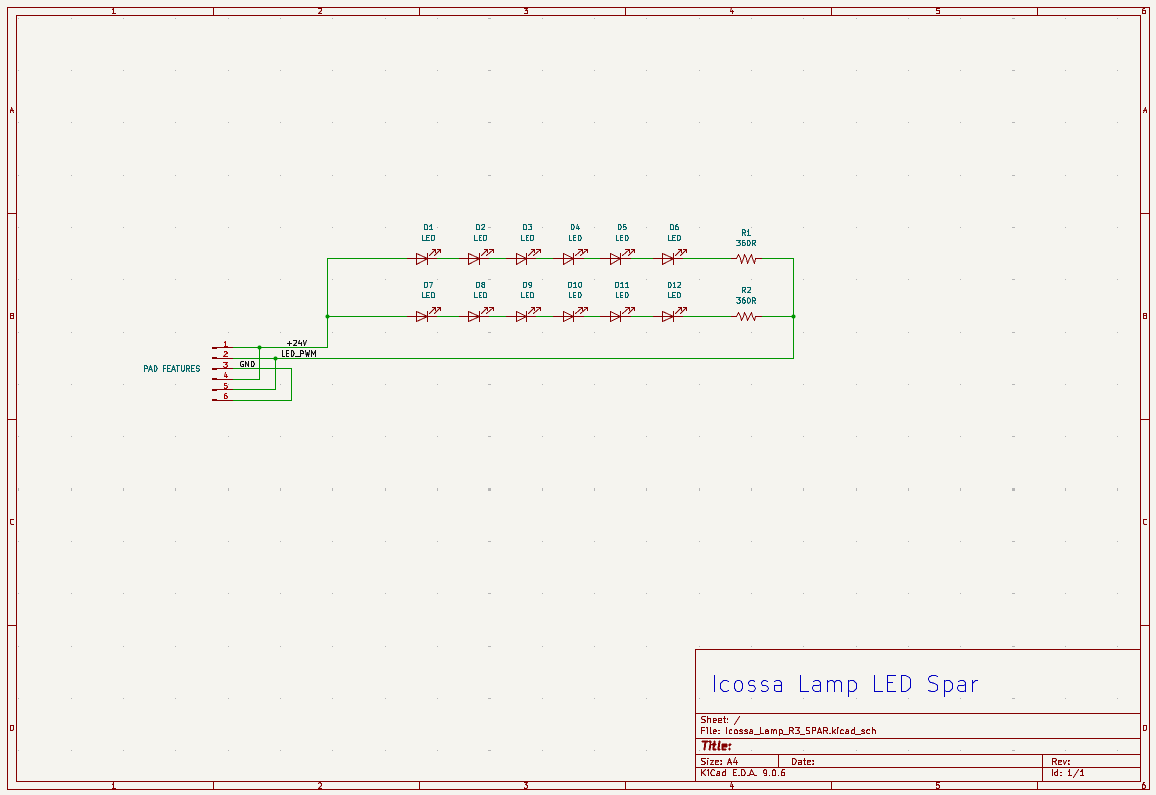
I am doing this design in Kicad, it’s my first time using this software.
It’s been an uphill climb, learning how to create arbitrary pad shapes and get them aligned properly has been a bit of a challenge.

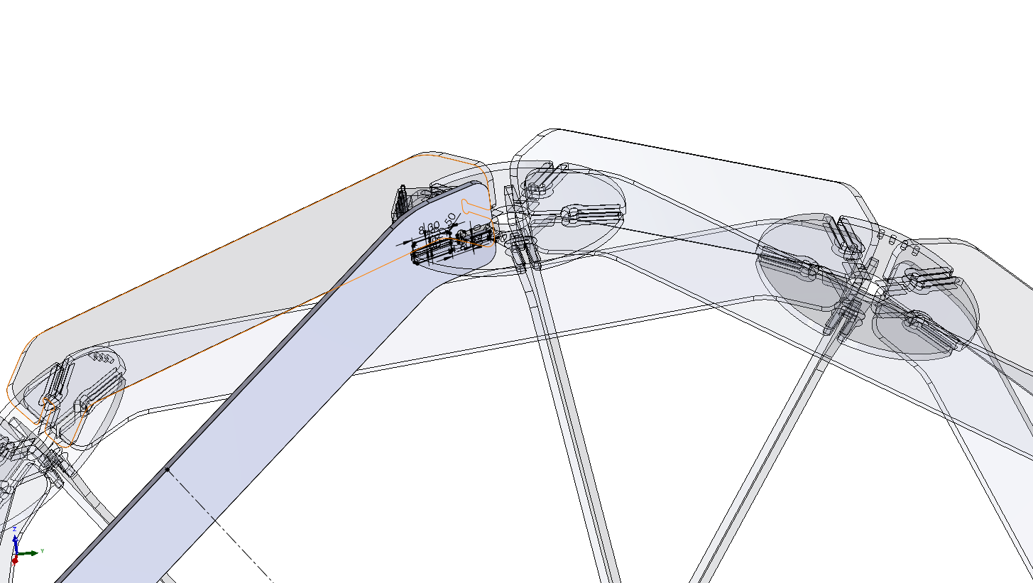
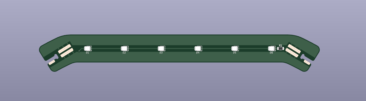
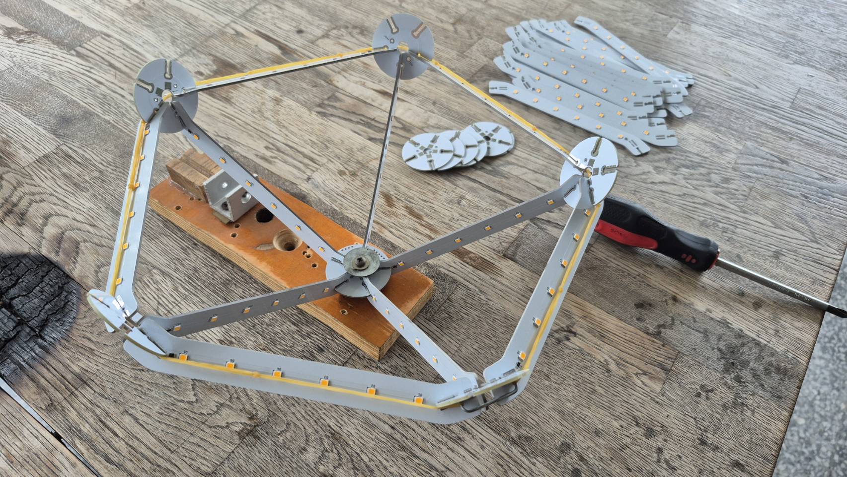
The PCB design for this lamp is a complex 3D puzzle, both mechanically and electrically.

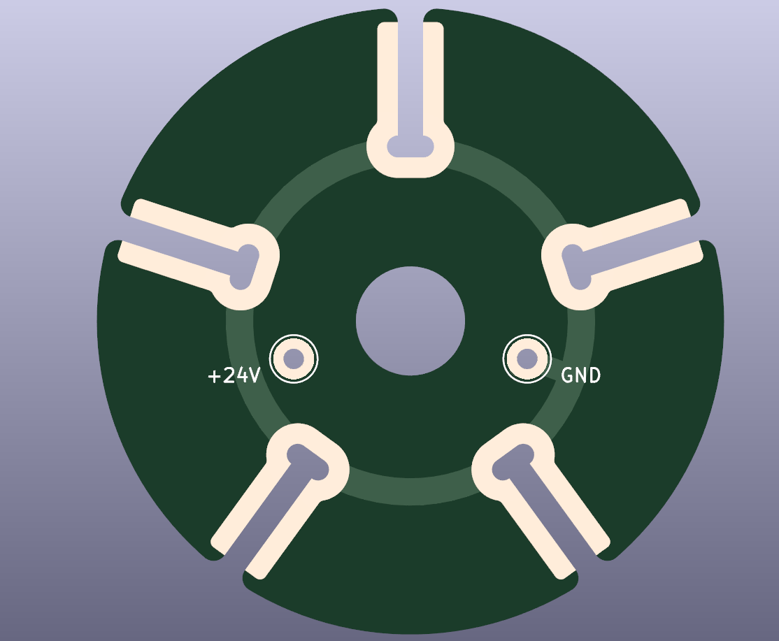
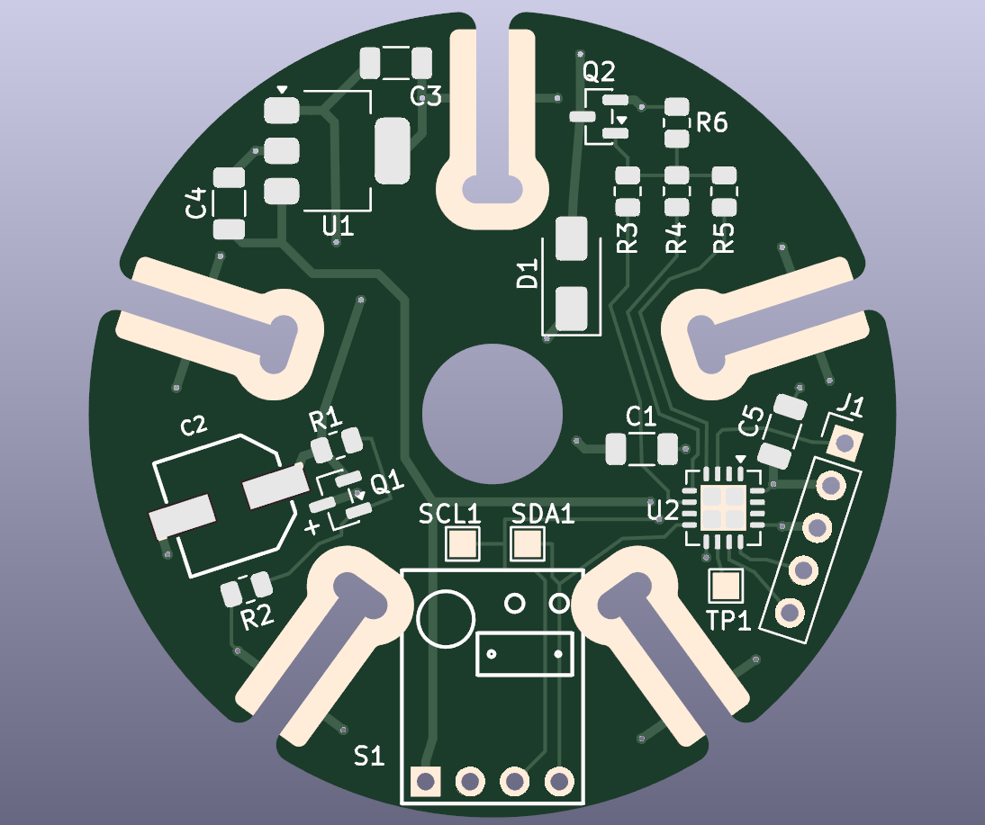
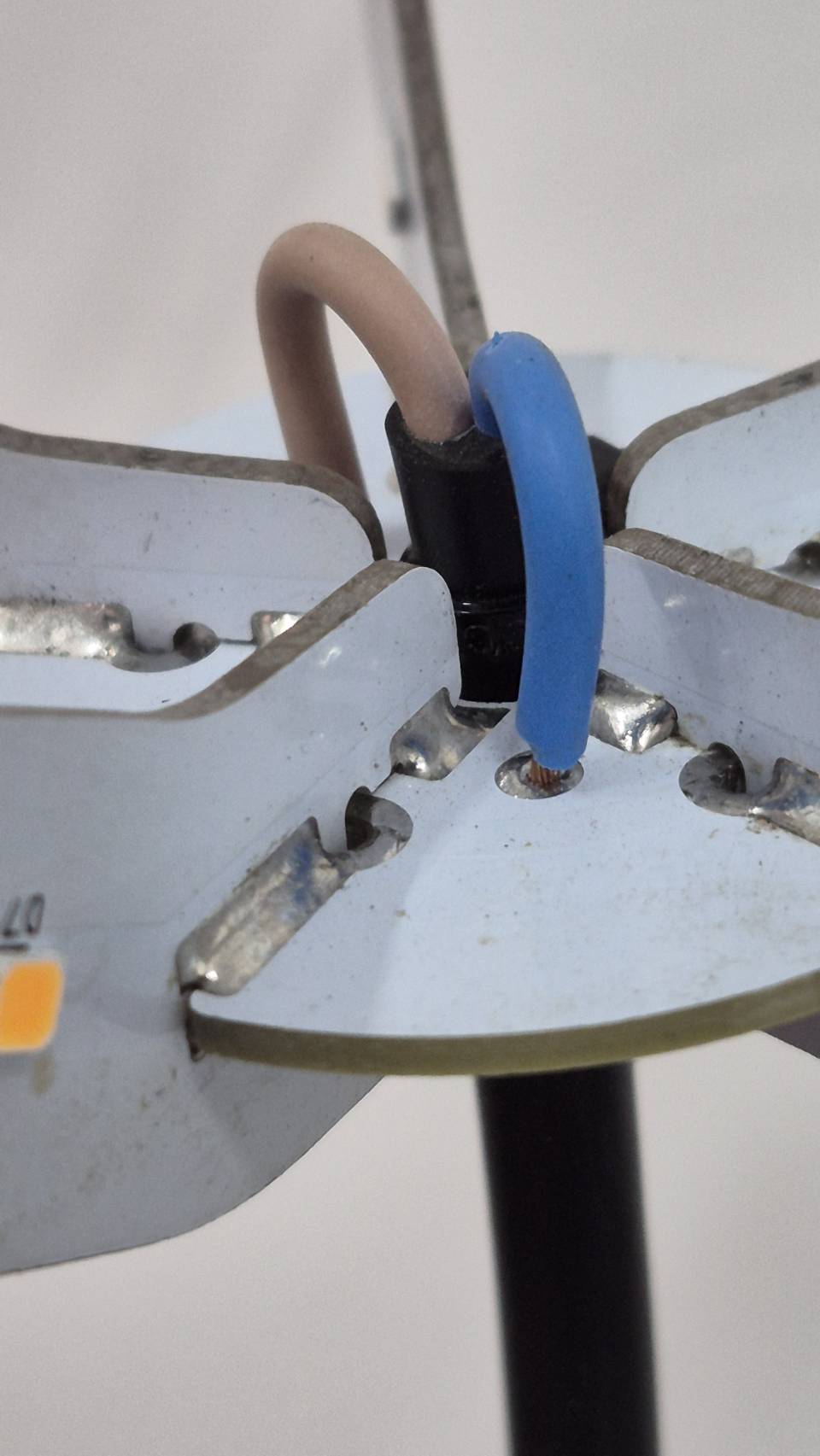
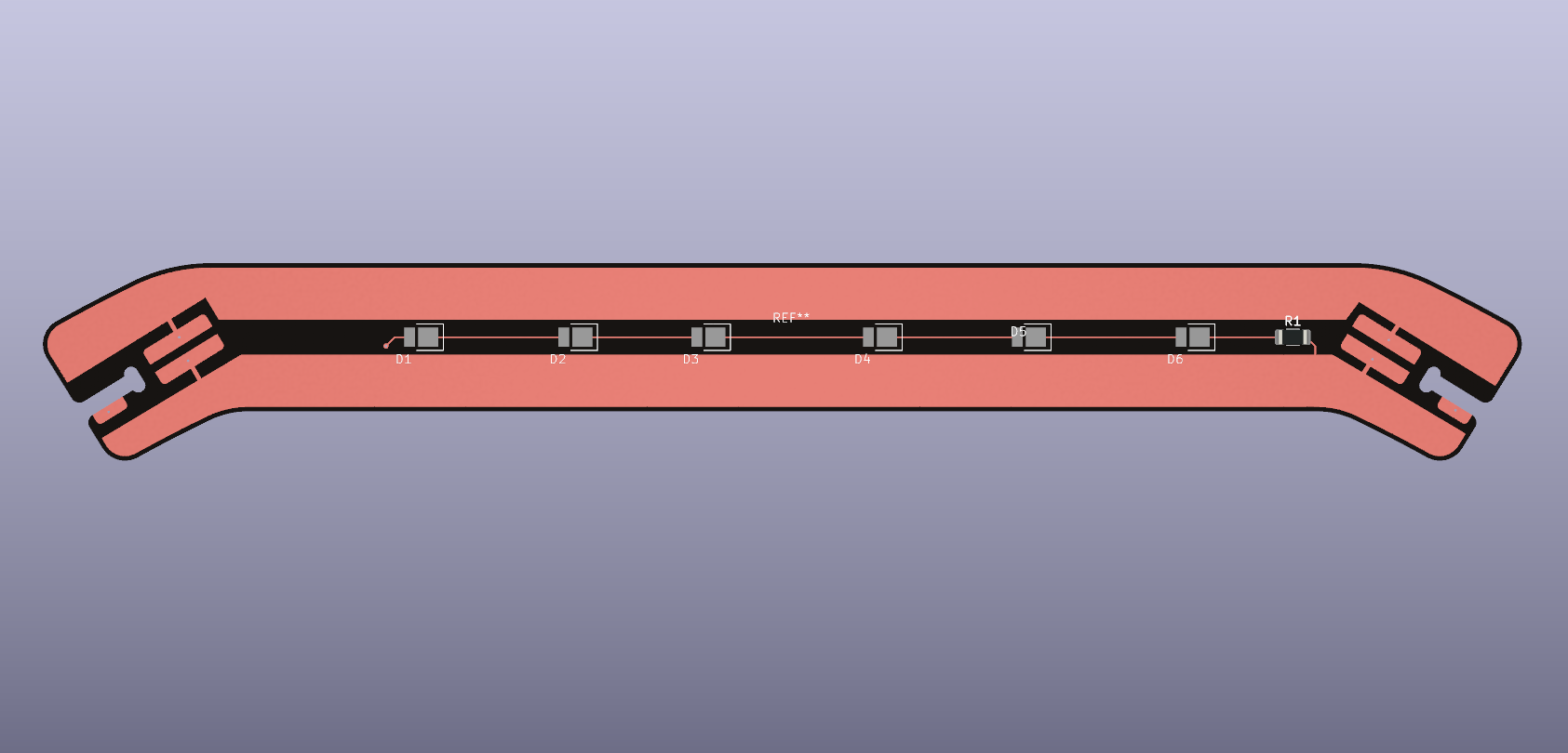
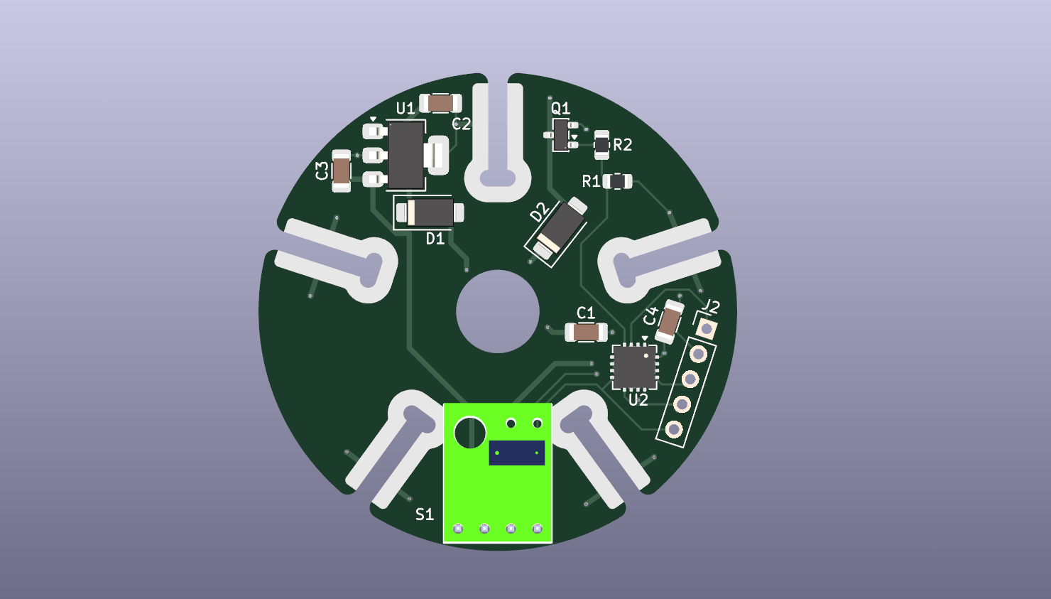
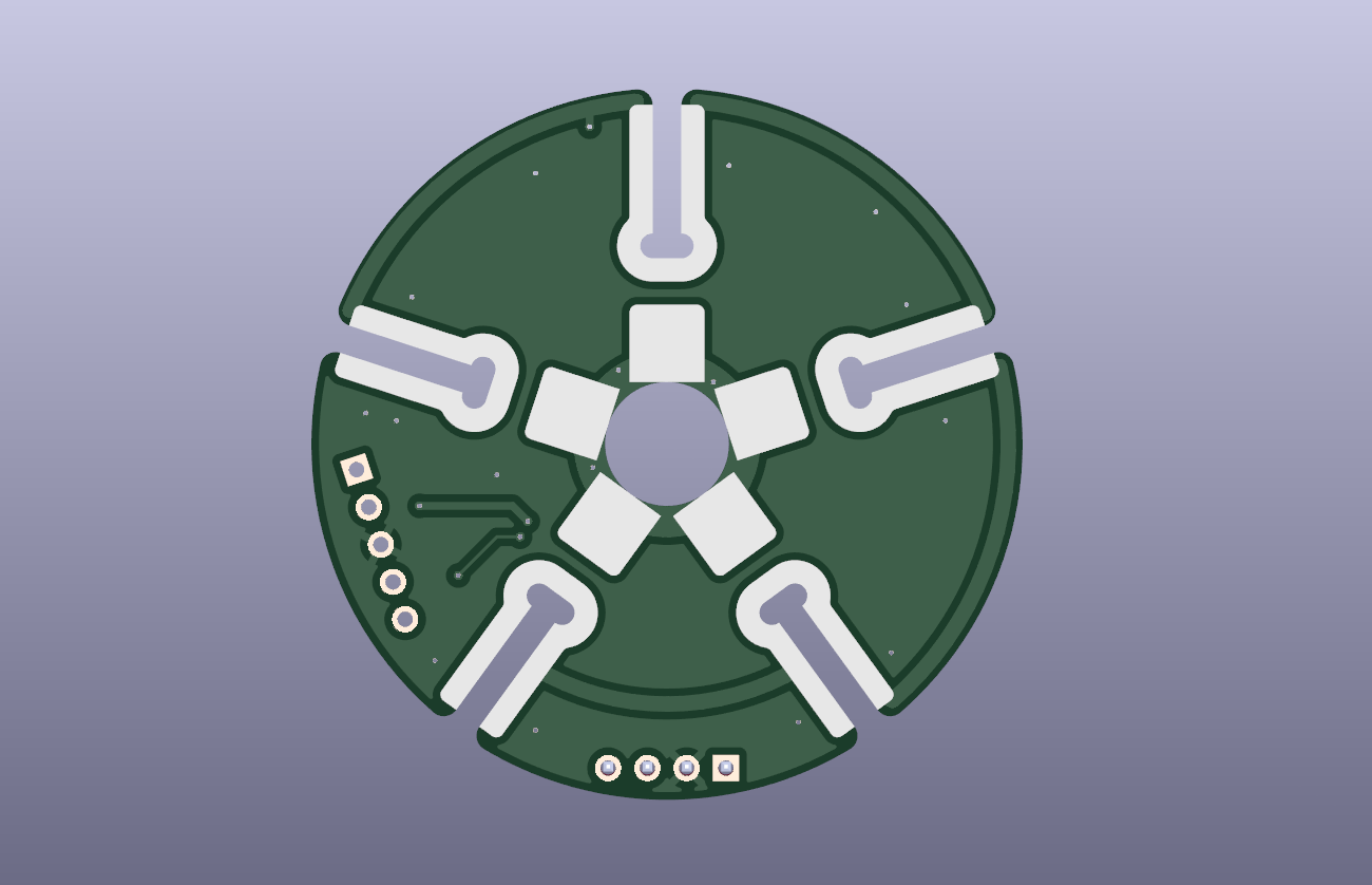
I modeled the pad geometry in Solidworks to get the size and alignment of the joints right, then exported the 2D geometry as DXF files. I then create pads in Kicad from the DXF files, linked to connectors on the schematics - so the netlist works correctly.

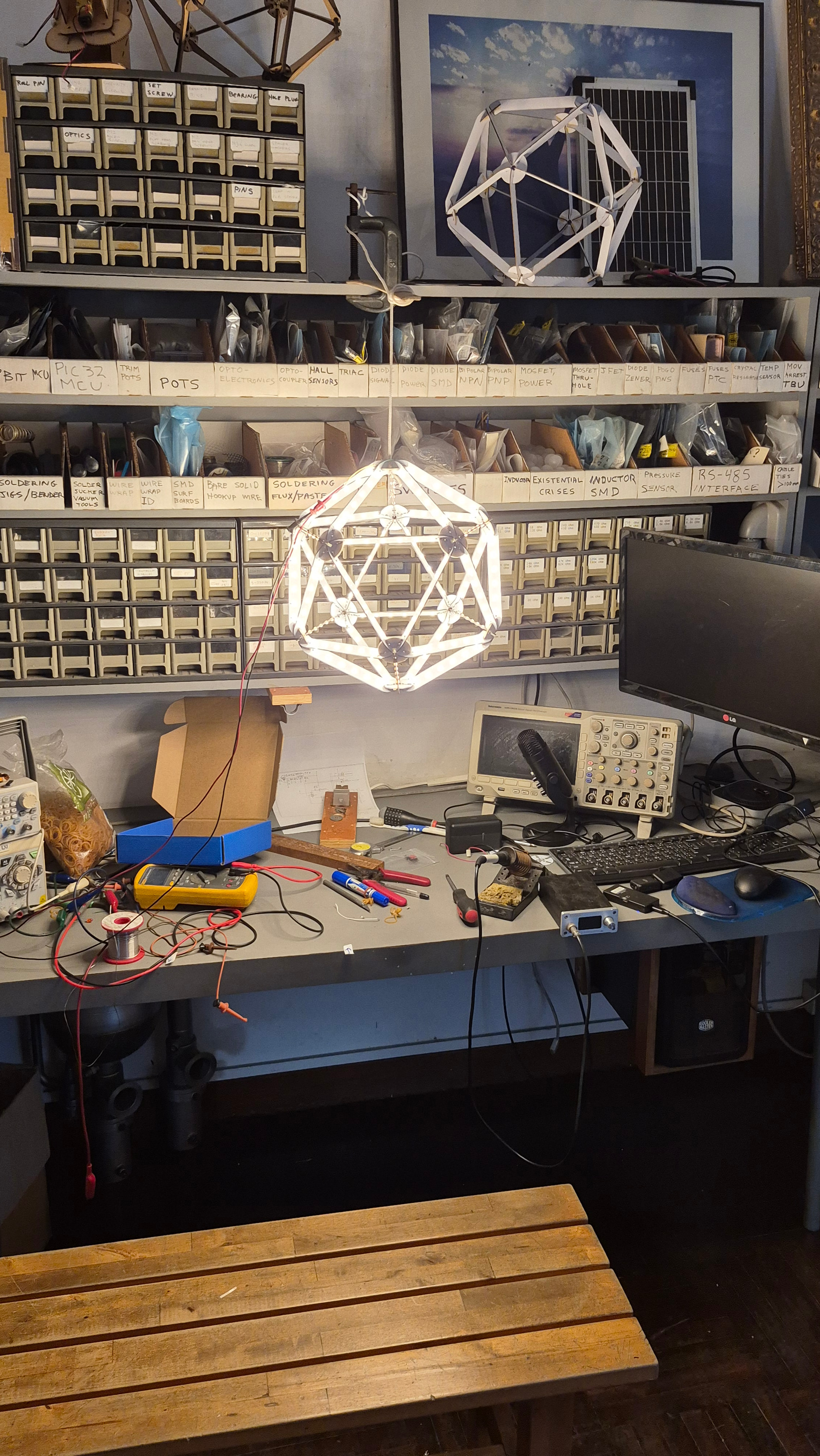
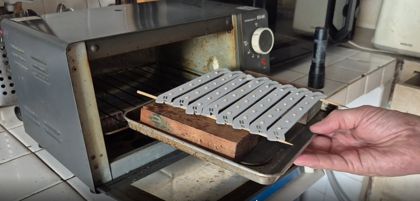
The cardboard mockup has been invaluable as a reference, it’s easy to loose track of where the connections are going when you look at the 2D screen, I marked up the cardboard with a felt pen to guide me along as I design.

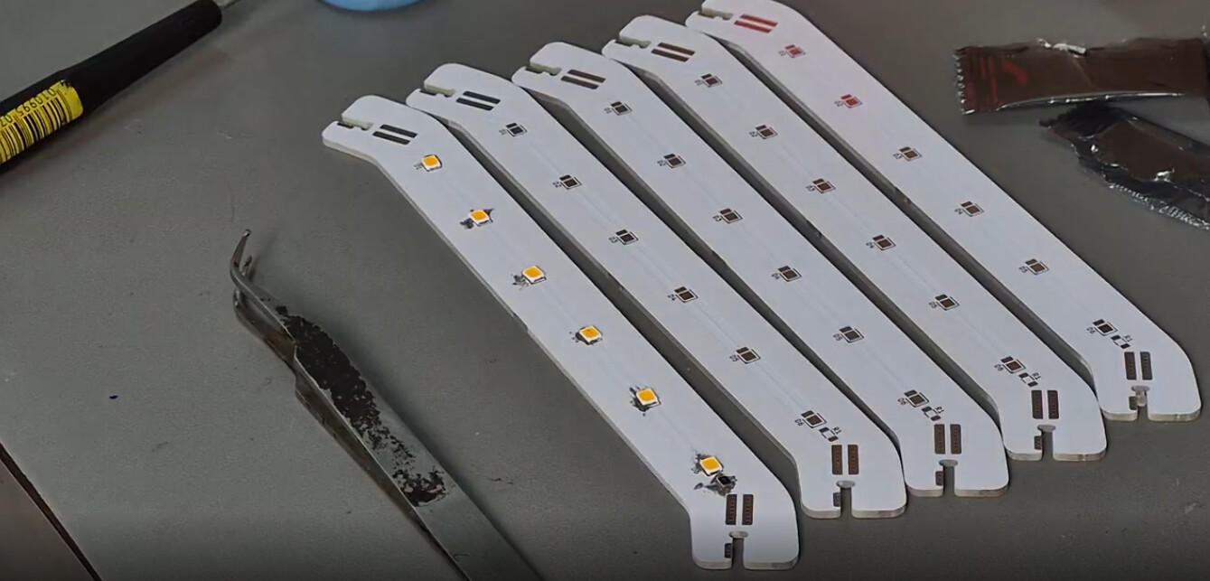
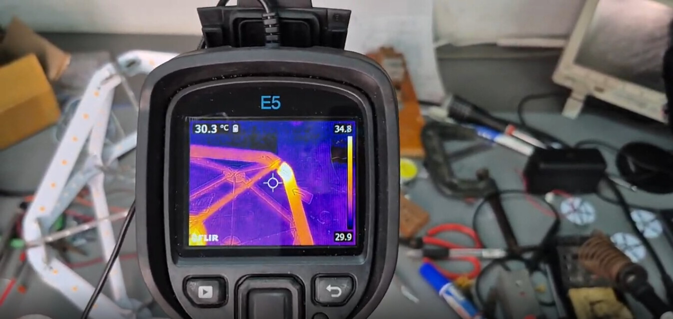
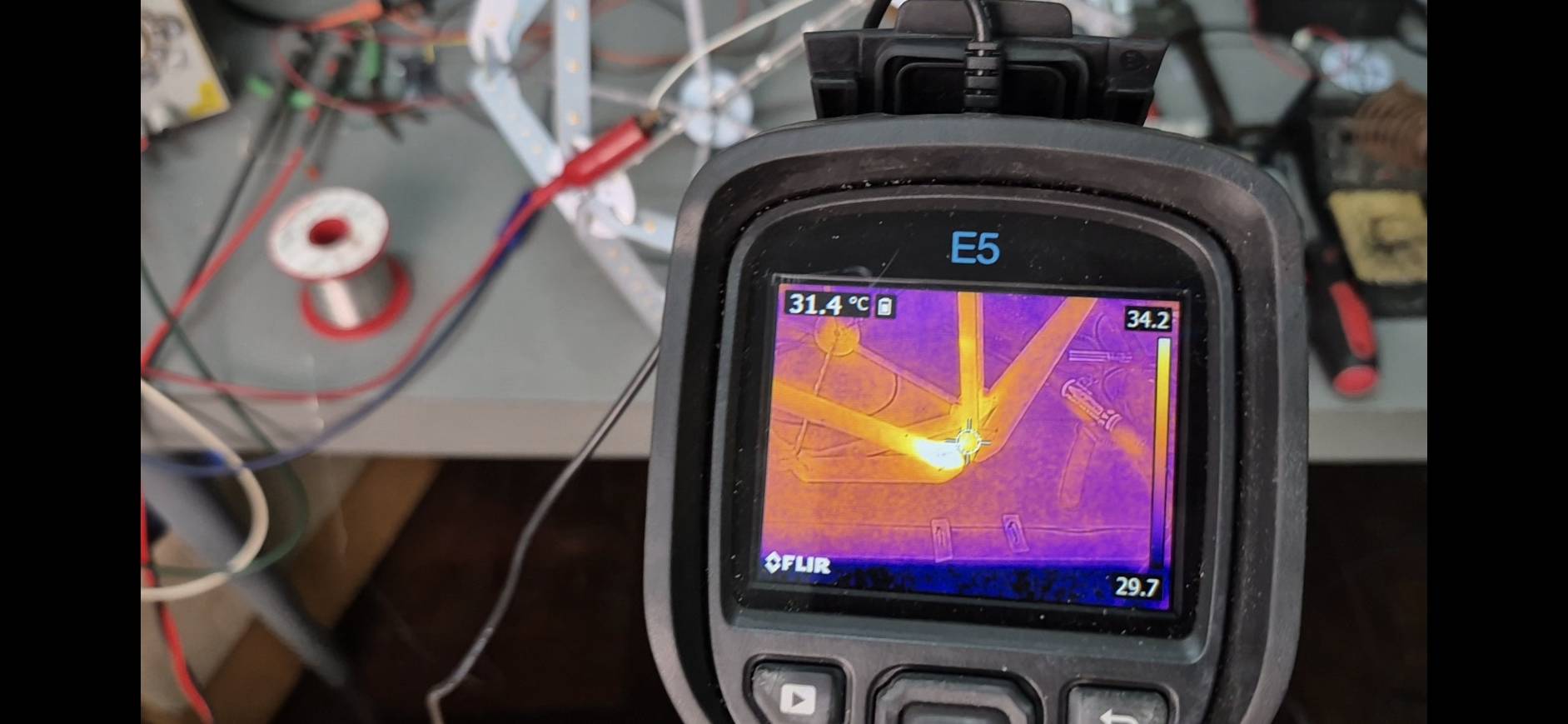
I am taking care to make sure all the joint pads are thermally relieved from the mass of the copper pours so they will heat quickly for soldering. The Spar boards have heavy pours to spread the heat from the LED’s out and provide low resistance circuit paths that also feature massive redundancy in the connections.

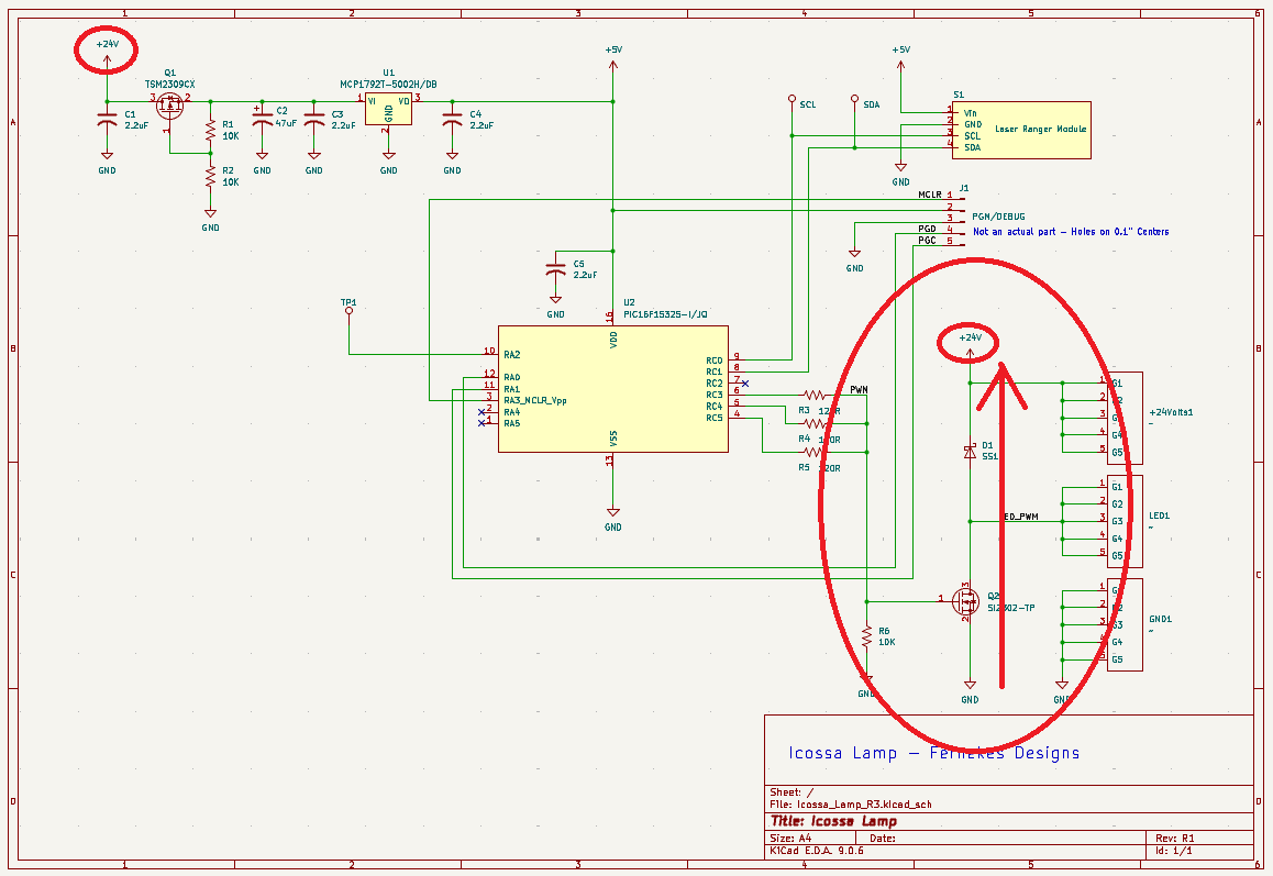
The outer edge of the entire icosahedron shape is GROUND - this should act as a nice static electricity path to prevent this open structure circuit from getting destroyed when people inevitably touch the lamp carrying large static charges.

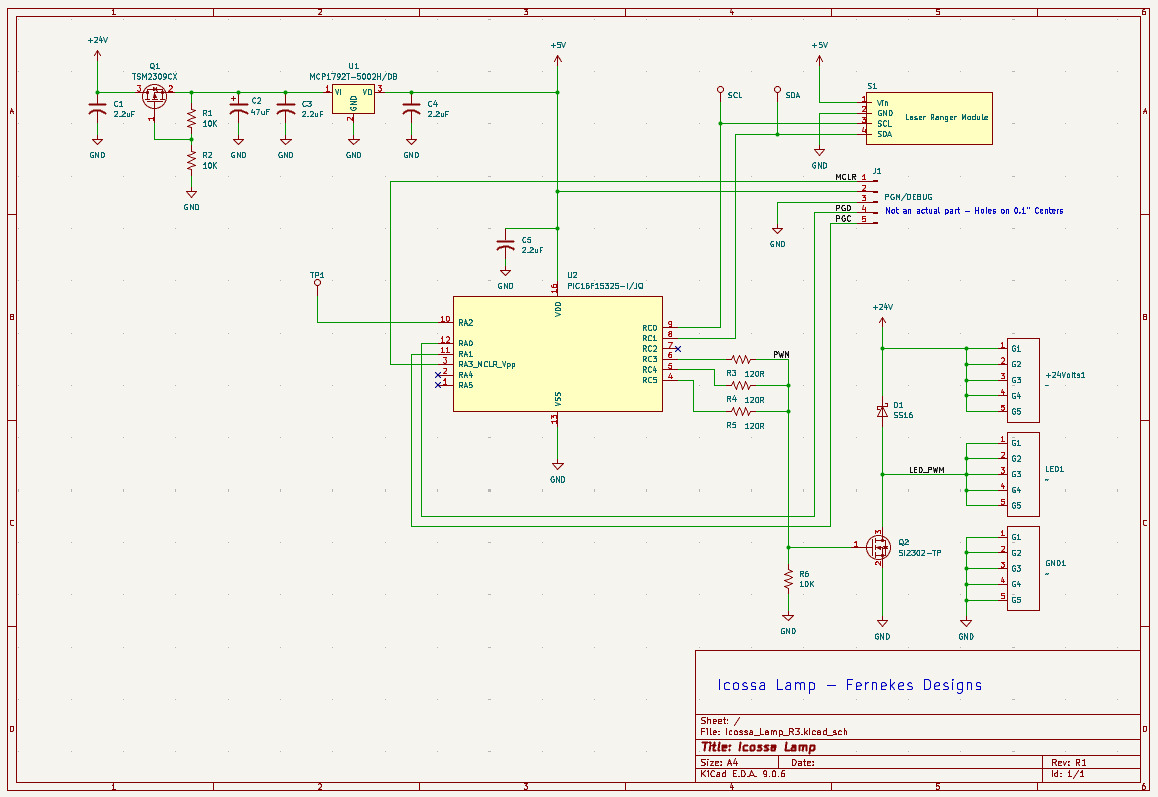
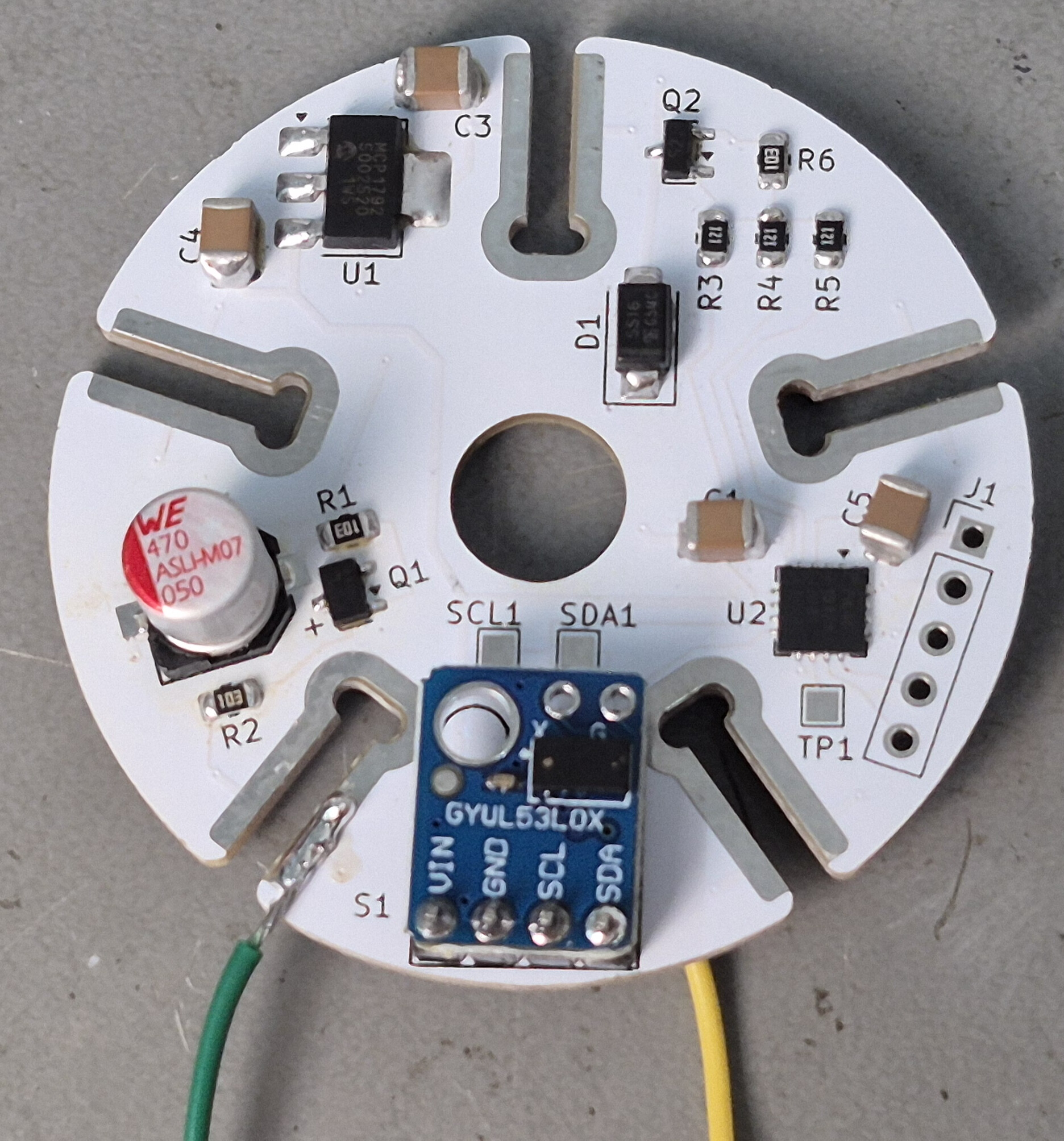
I have ordered parts from Digikey, first I will modify my hand-wired proto to match the new schematic and BOM, when I am satisfied that this works right, I will update the PCB and send it off for fabrication. I am taking the advice of Mikeselectricstuff - I will change the MOSFET to SI2302-TP, and changed the MCU to a PIC16F15325-I/JQ, with the idea of using paralleled IO pins to provide better drive for the MOSFET gate. (the original MCU does not have remappable IO pins)

I also decided to use an integrated sensor module which has a built-in voltage regulator and level shifters- the Vcc can then be 5V, another drive improvement and BOM simplification.

I’d be inclined to use more/thicker tracks from the solder pads as they could experience significant mechanical stress, and the foil adhesion may have been weakened from the soldering process. I’ve always been paranoid about this, but not sure how much of an issue it is in practice but costs nothing.

Yes- I agree- I think I will “stitch” the vias where I can.

On the Spar board, the net is the same on both sides. The hub board has different nets top and bottom in some places.

Finally - the boards are “in the soup” at JLCPCB.
They will be made in white Solder Mask with black Silkscreen.

I added via stiches to the Spars, these have the same net on both sides, the hubs have different nets on each side, it’s not really practical to stitch.

Each Hub is a power connection point - less to think about- more flexibility in application
This can be:
A hanging lamp - just wire a cable to the hub opposite the Master Hub.
A table lamp- rest it flat on a triangle, face the sensor up, or at an angle.
A floor lamp- Stick a lamp pipe to a vertical base with the lamp on top, sensor facing up.

Going to hand-assemble the first one, this is how i suffer and learn.
Next step is to panelize this and boil it down to two cracker PCB’s that can be pick-n-place assembled.

Scope for a few minor cost savings - I usually use the good old 7805 for the regulator, usually the SOT89. If you need small, there are plenty of obscure-brand SOT23 regs on LCSC for a cent or two.
No real benefit to using a FET vs. a diode for reverse protection as the current is low and you don’t really care about voltage drop here .

No programming header for PIC?

For QFNs that don’t need the die pad for heat or RF, I usually omit it, as it makes reflow/rework easier, and allows tracks under the chip.

Here is a quick demo of the Gesture Interface in action.
It’s working nicely, I think the ramping filter needs to be a bit slower acting.

Should I make the default Power On Reset state be with the lamp on? or off?
On is nice when you are installing it, and it can then be “controlled” by simply switching the power on and off.

The downside is that after a power failure, it will turn on, even if it was off before?

Here is the idea with the PFET-

(1) Note that the LED spars connect directly to the 24 volts BEFORE any polarity protection- they are diodes anyway- no problem here.

(2) I need a decent sized ‘Bulk’ capacitance on the 24V power line, so I am using an electrolytic cap, which DOES care about polarity, so this needs to be “behind” the polarity protection circuit.

Just using a diode here does not work- the capacitor is isolated, it cannot supply current to the bus powering the LEDs. The PFET effectively connects the capacitor to the power rail, but only when the polarity is correct.

This design choice is an artifact of the physical architecture of the lamp- the power comes in on the top, but the circuitry is on the bottom. This way I can keep the simple 3-wire connections through the spars, with the LED strings inherently protected, and hang a nice 47 uF electrolytic off the rail at the bottom, hiding safely behind the PFET polarity switch.

Great point about the QFN package! I will remember this one!

Here is my trick for PCB’s with PIC MCU’s- just make the PGM/DEBUG connection a row of 5 each 0.1” spaced plate-thru-holes in the PCB, when you need to program the MCU, take a header with square pins and ‘lean’ them over in the holes with a gentle pressure and it makes a solid contact. (the square edges bite into the edges of the holes, top and bottom) This has never failed me, and I love the zero cost and flexibility of placement. When I do intensive debugging, I just solder a pin header in place.

Neat subtle trick with the protection. Could be scope for a small optimisation though - as you have an NFET for the LED switch, you could save a BOM line by putting the protection in the -ve rail and using another NFET instead of the PFET.

I am obsessive about BOM minimisation - comes from running my own pick/place - I’ll happily use two or three 10Ks if I have them on the board and need a single 5K, 20K, 30K etc!

1 Like

Yeah! great idea!
BOM optimization can be a tricky trade off at times, but this is an obvious win.

Project update.

Got the PCB’s and have assembled a working unit.
It’s very nice looking and rather satisfying to play with.

I hand-soldered the hub together with an iron and hot-air gun.

The LED spar boards I soldered with paste and my trusty toaster oven.
It’s pretty sketchy, so I use low-melt solder paste so I can solder LED’s without destroying them in the process. I did both sides at once- none of the LED’s fell off!

Of course - there were shorts once I got it all assembled!
Initially I was very cautious, testing for shorts as I went along soldering, so I would know where to look if it did short.

It went so smoothly, I got cocky and blasted through the assembly thinking this was not going to be a problem.

And… short!

I setup my power supply to output about 5 amps (at a volt or two) and blasted the shorted circuit nodes to make the traces carrying current show themselves by heating up - it was actually really easy to find and fix the problem this way- without the FLIR camera, it would have been a bit of a nightmare. The thermal reliefs at the ends of the spar (to make it easy to heat with the soldering iron) are thin and have higher resistance than any of the other tracks, this makes the shorted joint light up very clearly - from the Infrared thermal perspective.

I fucked up the reverse polarity protection- I missed that the 24 Volt feed goes directly to the LED circuits - not through the reverse protect MOSFET Q1 (it protects the regulator and the electrolytic bulk capacitor only) when you reverse the polarity- there is a direct short through Q1’s body diode and D1- oops.

The solution is to replace D1 with a 24V rated bi-directional TVS diode.
D1 is there to clamp the Drain terminal against any stray positive over voltage. (ESD etc.)

A few other observations:

(1) The slots in the PCBs seem to be at, or near worst-case tolerance dimensions.
The fit is rather sloppy, which makes the assembly process more difficult, it all wants to fall apart in your hands. I don’t think there is much to be done about this- unless you want to pay more money to have the PCB house do the router work with higher precision.

(2) I think the key to making this easily is to assemble the entire shape together before soldering any of the joints! The use of rubber bands and paper clips to hold it together is advised. This way the lamp kind of “self-aligns” - which will avoid creating joint stresses as you build. I tried to do the assembly as two halves, which was rather difficult as the joint fit is s sloppy, some of the hubs did not align perfectly- you can barely see it, but it bothers the anal retentive- like me.

(3) Must fix the reverse polarity design problem.

(4) A few parts on the Hub board could be moved to make it easier to get in and solder the joints.

(5) I want to change the design of the solder joints a bit.
Overall it’s really quick and easy to solder these together- but it’s a LOT of soldering! if you count each individual solder pad - it’s 360 solder operations!
The fact that I had 2 shorts is the problem, these seemed to happen most where two nodes are directly on opposite sides of the Hub board. This also means I could not apply via stitching at these points, which dramatically toughens the copper- it simply cannot peel off if you stitch the pads with a dense grid of vias.
I will want to stagger the joints, this will allow stitching and make any shorting really easy to see visually. (the shorts I had were impossible to detect by inspection)

(6) There is one strange behavior: The lamp will randomly turn on or off by itself when left unattended!?

At first, I thought it was just responding to the insects that are inevitably attracted to the light, but now I have seen it switch with NOTHING in the sensing area. I will need to setup the scope and monitor the lamp- I think the sensor glitches from time to time, I can filter this in code if I can get a handle on what this actually looks like in the signal domain.

I am going to work on the final video for this next.

Hi Leo,

We have a bank holiday here on 3rd April for Good Friday (Easter).

Do you think it’ll be possible for me to order some board or get some boards made that I can assemble that weekend?

A lot of “ifs” - but sure? The PCB’s can be had in less than a week

Do you have the capability to do the SMD soldering?
It took me about 6 hours to build mine- doing everything.

If you want to build one- let me know and I will fix up the files and put them up on Github.

Hi,

Thanks Leo.

Yes, I have iron, air and plate so am happy to take on the soldering.

I’m happy to order my own boards or buy them from you, whichever is easier or works better for you.

Does the BOM come from a single supplier such as Mouser, Digikey, RS or Farnell?

I have the capability to program an AVR but am not so familiar with the PICs. I might be able to arrange some kind of PIC programmer, but I don’t (currently) have the PIC toolchain (Linux) so a binary or hex file would be handy for that.

Any assembly instructions would be a boon as well! :slight_smile:

I will prepare the files today and up load to Github for you.
Here are all the files needed.
I have fixed the issue with reverse polarity protection and moved some parts to make assembly easier.

Order the 3 PCB’s (Hub_Power, Hub_Master and SPARS)
(open the BOM file to check the quantities of boards needed)
Order the parts from the BOM list - Digikey has all of them.

Here are my hints to a smooth build:

(1) Assemble the Spar boards first.

I used paste and a toaster oven, soldering both sides at once.
Test each one - make sure the LEDs work on both sides
Clean the boards with IPA- it’s much easier when they are flat.

(2) Build the HUB_Master PCBA
Program the chip with the .HEX file.
Make sure it works by soldering a LED with a 1K resistor to the pads.
(Anode to +24V and Cathode to LED Output- See PDF Hub Connections)
You should be able to control the single LED with the sensor.

Hub Connections.pdf (866.8 KB)

(3) Assemble the Icosahedron shape using rubber bands and paperclips to keep it all together. It self-aligns really nicely this way, the boards tend to naturally find the right position, supported from all directions. I started with a block of wood and a screw to hold the thing down so I could work on it comfortably.

The Master hub goes in with the components on the outside of the icosahedron.

Be sure the power hubs are right-way-out. - so you can read the legend on the silkscreen, (+24V and GND) from the outside.

DO NOT be tempted to just start soldering the boards together one by one, you will end up with a poorly aligned mess that will stress the solder joints and cause general unhappiness.

Once you have the shape assembled, go around and tack-solder it until it’s totally locked together, take care to make sure the pieces are bottomed in the slots and the hubs are perpendicular to the spars. do one little tack solder per spar, just to hold it together.
Re-melt and adjust if things do not look right.

Now remove the rubber bands and continue the soldering operation.

Missing a joint or two is not a big issue as there is massive redundancy in the connections.

Beware of shorting the LED_OUT net to the GND net with sloppy soldering, I did this a few times and had to use my IR camera to locate the offending joint. I blasted the short with about 5 A to make it light up thermally, easy if you have the tool…

Attach a cable to the power hub opposite the Master - here is how I did it:
A cable tie around the cable acts as a stopper, taking the strain off the wires.

Enjoy.

Hello again!

I’m nearly ready to order everything.

The gerbers all look good in JLCPCB. I looked at getting them to do a panel as it used to be cheaper for things that were less than 100mm x 100mm but the only saving was for the cost of deburring the boards and I think that’s worth the 70p!

I uploaded the BOM spreadsheet to Digikey’s “myLists” tool and it found all the parts except the GY-VL53L0XV2. I had a search around and there’s something with that name on Amazon but it looks different to the one in your picture earlier in this thread. https://www.amazon.co.uk/GY-VL53L0XV2-Flight-Distance-Measurement-Measuring/dp/B07VG8NX8Q

Are you able to suggest a source?

If all goes well I’ll place the orders for everything tomorrow.

There seems to be 2 different styles of these breakout boards:

This is the one you want- small rectangle with NO EARS

These with the mounting ears WILL NOT FIT
Don’t buy these.

There are many available from China for $1 or less?
UK is another story?

AliExpress has them:

Hello again,

The ToF sensor arrived last week some time and the boards arrived yesterday.

The first impression when I saw them in real is that there really is a lot of boards! They’re also quite weighty. And even tho’ the spars are small, I think this thing is going to be quite large!

There’s a fair bit of slop in the joints between boards. My calipers measure the thickness of the spars at exactly 1.6mm. The gaps in the hub measure somewhere between 1.83mm and 1.94mm. I’ll assemble it with the elastic band trick you recommend.

I haven’t put the DigiKey order in yet as I’m still sorting out a few more components for another project.

I’m looking forward to the construction tho’. :slight_smile:

It’s going to be a showstopper once it’s built.

How’s yours holding up?

Mine is working great- once you solder this thing together, it’s really robust.
I feel like it could withstand quite a bit of kicking around.

The tolerances of board thickness and router accuracy demand a sloppy fit - it could be tightened up a bit- but it would be a nightmare if it ended up on the too-tight side.
I used published tolerance specs to design it so it will always fit- but it would be nice if it was tighter!

Resist the temptation to start soldering the boards together before it’s in the final shape!
This is the key to a nice outcome!