Learning Objectives
- Understand CMOS IC characteristics, power requirements, and advantages over TTL technology
- Build and test Schmitt trigger circuits to observe hysteresis behavior and noise immunity
- Develop systematic troubleshooting skills for breadboard circuits and component failures
- Use oscilloscopes for waveform analysis, triggering, and frequency measurement of oscillator circuits
YouTube Video
Unedited Video

Timestamps
- 0:00 - Introduction to CMOS technology and CD4093 quad NAND gate overview
- 1:26 - CMOS vs TTL comparison and voltage range advantages
- 2:44 - CD4093 datasheet analysis and Schmitt trigger symbol identification
- 4:45 - NAND gate truth tables and logic gate construction techniques
- 13:39 - Power supply connections, VDD/VSS pinout, and chip orientation
- 18:25 - Circuit protection, polarity safety, and bypass capacitor importance
- 26:00 - Potentiometer wiring and voltage divider configuration
- 37:32 - Systematic troubleshooting methodology using multimeter measurements
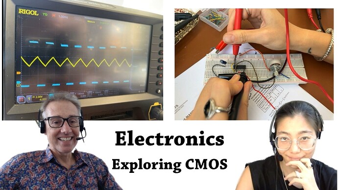
- 1:14:16 - Oscilloscope setup, probe configuration, and hysteresis visualization
- 1:39:43 - RC oscillator circuit construction and capacitor-resistor feedback
- 1:45:51 - Waveform triggering, time base adjustment, and frequency measurement
- 1:56:31 - Manual vs automatic frequency calculation techniques
PDFS
CD4093B Datasheet - Official CMOS Quad NAND Schmitt Trigger Specifications (1.0 MB)
Basic 2-Input NAND Gate Circuit with Truth Table (395.6 KB)
NOT Gate Logic Circuit Implementation (272.2 KB)
AND Gate Circuit Using NAND-NOR Configuration (370.7 KB)
OR Logic Gate Circuit Implementation (374.1 KB)
XOR (Exclusive OR) Gate Circuit Configuration (409.5 KB)
Schmitt Trigger Test Circuit with Input-Output Probes (186.8 KB)
Current Sourcing Circuit with LED Output Indicator (124.2 KB)
Current Sinking Circuit with Diode Output Configuration (181.1 KB)
Gated RC Oscillator Circuit with Enable Switch (158.6 KB)
Falling Edge Detection Circuit Implementation (141.5 KB)
Rising Edge Detection Circuit Implementation (100.7 KB)
XOR-Based Edge Detector Circuit Configuration (220.1 KB)
Technical Definitions
CMOS “Complementary Metal-Oxide-Semiconductor”
Low-power digital circuit technology using complementary transistor pairs.
Works over wide voltage ranges, slower than TTL but very efficient.
IC “Integrated Circuit”
Electronic circuit with multiple components fabricated on single chip.
Contains transistors, resistors, capacitors in miniaturized package.
CD4093
Quad 2-input NAND gate with Schmitt trigger inputs in 14-pin package.
Part of 4000 series CMOS family, versatile for logic circuits.
TTL “Transistor-Transistor Logic”
Digital circuit family using bipolar junction transistors.
Faster than CMOS but consumes more power, common in 1960s-70s.
NAND Gate
Logic gate outputting LOW only when both inputs are HIGH.
Fundamental building block capable of creating any logic function.
DIP “Dual In-line Package”
Rectangular IC package with two parallel rows of connection pins.
Standard format for through-hole mounting on breadboards and PCBs.
Schmitt Trigger
Input circuit with hysteresis providing noise immunity and clean switching.
Has different threshold voltages for rising and falling transitions.
Truth Table
Chart showing all possible input combinations and corresponding outputs.
Essential reference for understanding digital logic gate behavior.
VDD “Voltage Drain to Drain”
Positive power supply connection in CMOS circuits.
Derived from MOSFET drain terminal naming convention.
MOSFET “Metal-Oxide-Semiconductor Field-Effect Transistor”
Voltage-controlled transistor used in CMOS digital circuits.
Building block of modern integrated circuits and processors.
VSS “Voltage Source to Source”
Ground or negative power supply connection in CMOS circuits.
Complements VDD to provide complete power supply for chip operation.
Breadboard
Solderless prototyping board with interconnected tie points.
Allows temporary circuit construction for testing and experimentation.
Oscilloscope
Electronic test instrument displaying voltage waveforms over time.
Essential tool for analyzing signal timing, amplitude, and frequency.
Probe
Test lead connecting oscilloscope to circuit measurement points.
Includes ground clip and signal tip for accurate waveform capture.
Hysteresis
Property where switching thresholds differ for rising/falling transitions.
Provides noise immunity and prevents oscillation at thr