Simple LED strip Dimmer/Controller

Everyone loves a good LED strip to add light in that special spot in your home.

LED strips are available in many forms to suit almost any taste or application, and they are really cheap and good these days.

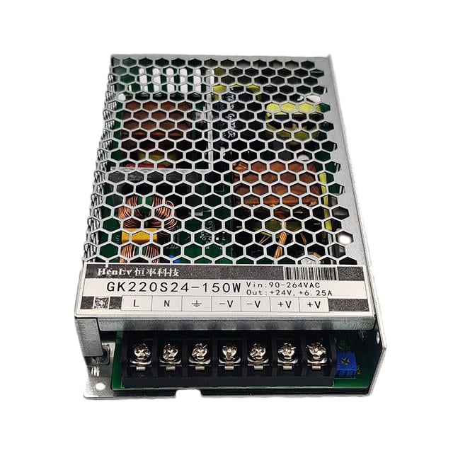
Powering these is a simple matter of buying an AC to DC power supply, with the output voltage and power matching the LED strip - cheap and easy to find.

Things get more complicated when you start considering how to install this stuff- especially if you want to dim the lights, and control them from a remote location - which is almost mandatory for most applications.

There are many ways to accomplish this, but most add significant cost and complexity to the simple concept mentioned at the start.

The most expensive part is usually installing the wiring, and this gets really painful if you are trying to retrofit this hardware into an existing lighting circuit, you inevitably need to add more wires and spend A LOT more money…

Unless… of course, you went for the wireless IoT controller thingie or the cheap Chinese dimmer with the IR remote control - all of which implies subtle, annoying compromises.

It’s my personal philosophy to avoid all that IoT home automation stuff, it just adds layers and layers of complexity, and when it stops working, you are in for a hellish troubleshooting session. Not to mention all the security problems associated with hanging this crap on your network!

When your friends come over to house sit, they cannot turn the lights on without calling you 5 times to finally figure out how to download the app to control the system.

The IR remote sort of works - unless you cannot place the receiver box within line-of-sight in the room, and let’s not forget to change the battery, oh and WHERE did you see it last?

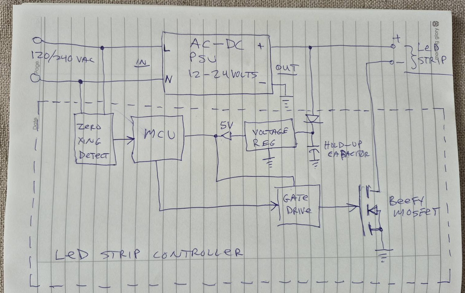
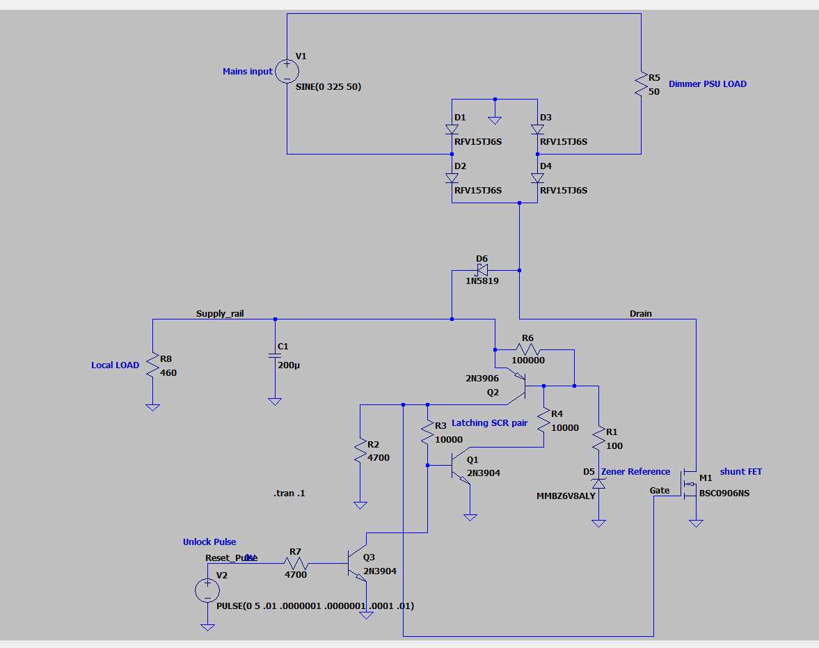
Here is my simple idea-

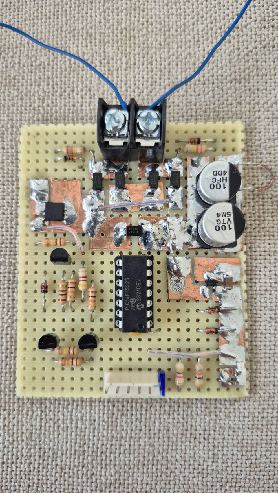
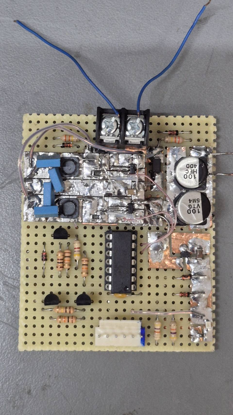
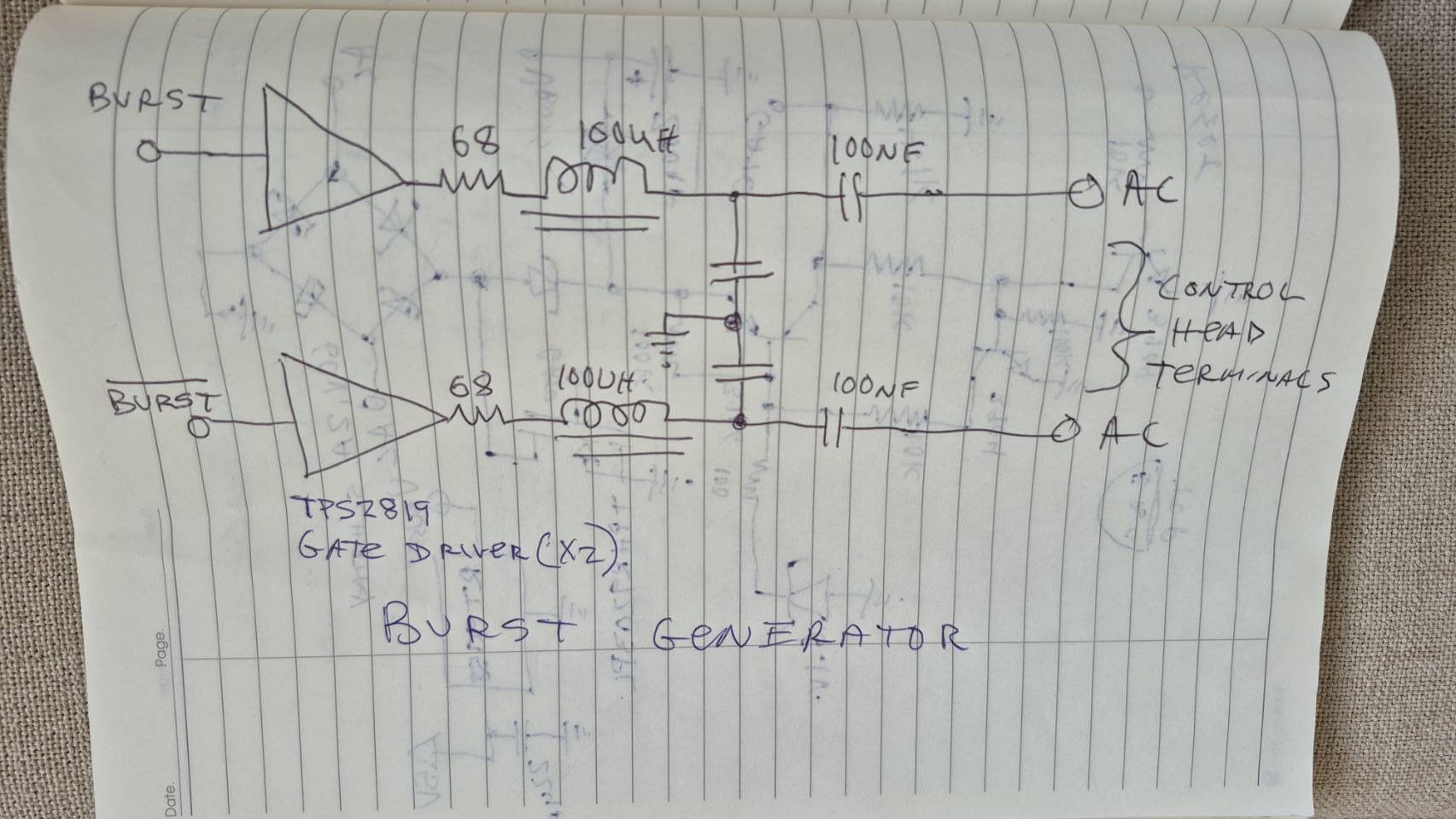
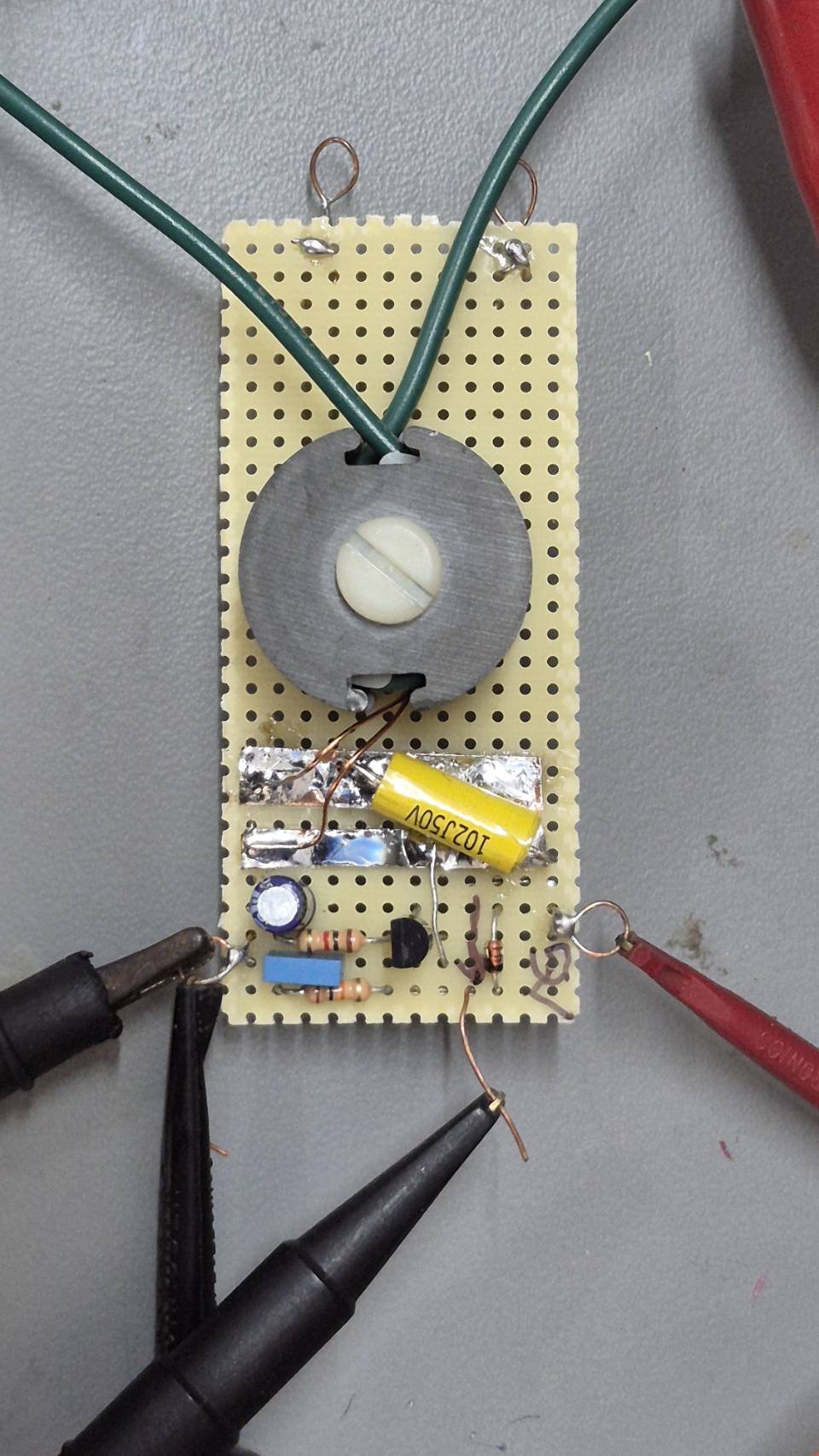
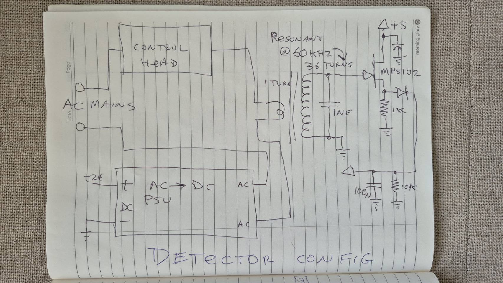
This little board sits with the PSU, it’s powered by the DC output.
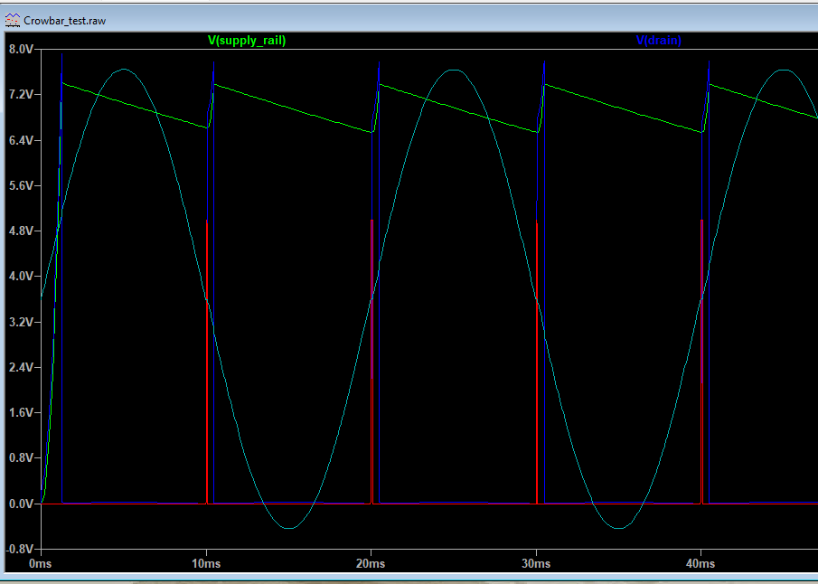
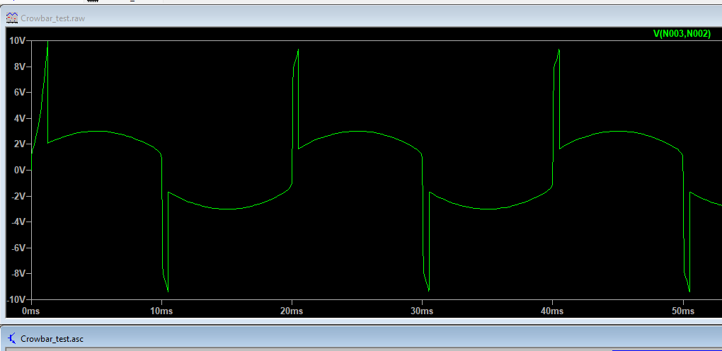
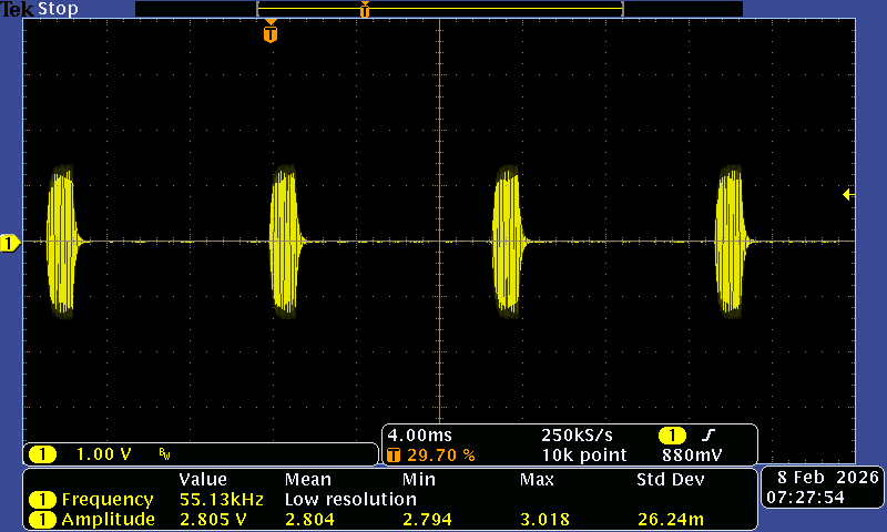
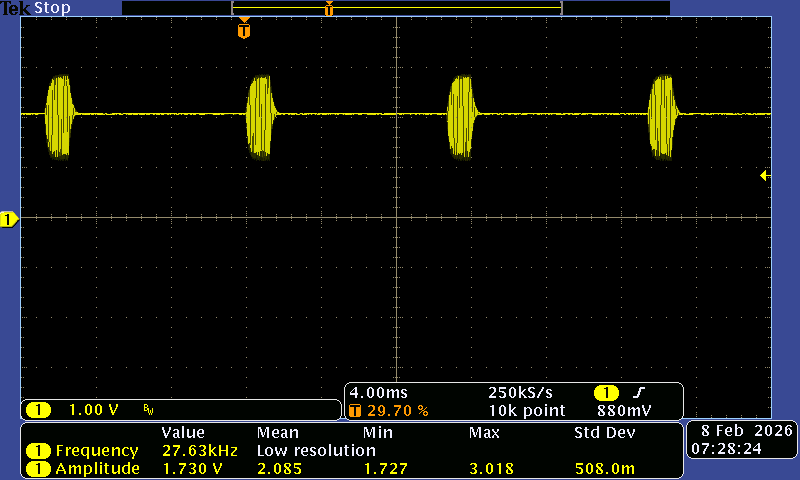
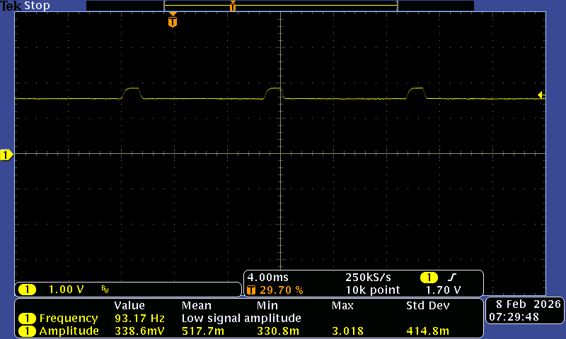
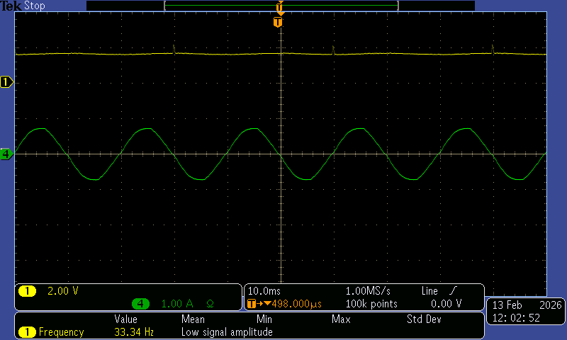
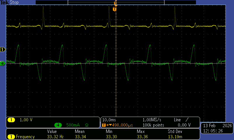
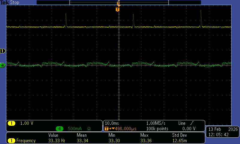
An isolated zero-crossing detector monitors the state of the incoming AC line, when it detects a voltage drop-out, it changes to the next state. The PSU’s internal capacitors and the hold-up capacitor should keep the board alive for at least 3-4 seconds after the power fails.

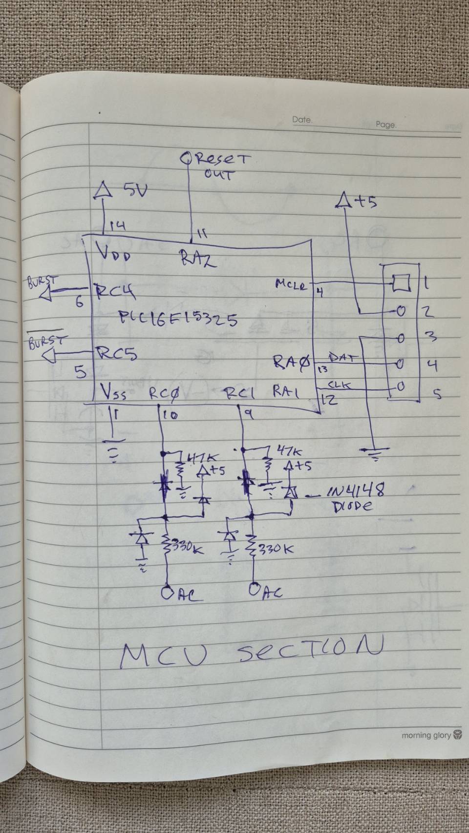
When you power this up cold, the unit immediately lights the LED’s to a low brightness via PWM, the brightness increases steadily over about 15 seconds to FULL-ON. If you flick the power switch on-off-on during the ramp-up period, it simply holds that last brightness level, if you do nothing, it just ramps to full brightness. turning it off again resets to the beginning.

This all sounds a little awkward, but I have a version of this working in my living room, it’s simple and easy once you get the hang of it.

(1) You can use the existing wiring and switches- no extra control wires are needed.
(2) It’s really cheap- you don’t need any bespoke dimmers or control boxes- besides this tiny simple board.
(3) Any person can always turn on the lights - even if they have no idea what is going on.
(4) No parasitic power is consumed- when it’s off - power consumption is ZERO.

I imagine this built into a little plastic box with terminal strips on each end:
2 terminals for the mains input, on the other side, 4 terminals- DC in and LED out.

Sounds cool!

A friend was telling me about a protocol for dimmable LED bulbs that involves encoding some data at the beginning of the 50/60Hz sine wave. I don’t recall if it has a name or is specific to a certain vendor.
Because LED lights can get to full brightness without using the whole cycle, you can use dead times with specific lengths at the start of the cycle to encode specific information such as dimmer level or colour temperature. In the absence of such information, you can still use trailing edge dimming with a regular dimmer unit to control the brightness of the bulbs.

It might be cool if your circuit above worked as you described by default but could also be paired with a replacement switch on the regular wall plate that could select different modes or configurations more naturally.

There’s some challenges to overcome in UK configurations where permanent neutral is not always (or even usually) available at the switch location but for the kinds of control you are describing, I don’t think this will be an issue, especially if there’s a bit of EEPROM or user flash in the controller in the switch.

Your point about the availability of Neutral is the elephant in the room, that’s the big problem, how do you power the dimmer control head without needing extra wires…

As you mention, It seems like there should be a way to use the portion of the cycle near the zero crossings to both power the dimmer control head and convey a few bits of brightness value to the actual load dimmer.

For my thought experiment, I am going to assume that at the control location, all we have available is (a) a Hot wire, and (b) a wire running to the load. At the other end, the load side, we have a Neutral and the switched Hot. (typical situation)

It’s a super challenging design problem- love it.
I am going to think about this and see if anything sticks.

Regarding the availability of neutral, do you think it’s acceptable to occasionally leak a little current into the load to charge a capacitor (or super capacitor or battery)? That would allow us to develop a power budget for the dimmer head. When the load is supposed to be switched on the dimmer head could charge and if it’s off for “too long” (perhaps a day?) then it could leak a little?

Solutions do exist that involve installing a capacitor across the load but it would be nice to explore alternatives.

However, I was assuming that the dimmer head would remain pretty simple: your original design has a regular switch. A simple extension would retain the switch or have a dimer knob with a switch when turned all the way anti-clockwise. If you avoid displays or indicators on the dimmer head then any UI can connect power to the load and then transmit the data as the light will be coming on anyway. i.e. I think it’s feasible to design a reasonably advanced dimmer head that only requires power when the load is (supposed to be) on.

Here is the AC line current feeding a 75W, 24V PSU (Meanwell NES-75-24) when loaded at about 30 watts. (heavily averaged to clean it up)

The power factor is obviously pretty crappy, the majority of the power consumed happens in big spikes recharging the main energy storage capacitors.

It seems like there is plenty of “room” to do stuff around the zero crossings that would have almost zero impact on the power delivered to the DC output.

Here is the same setup- with a really light load- maybe 2 or 3 watts.

If we think of the whole mains-dimmer-PSU circuit as a loop, we can manipulate this circuit around the zero crossings to do some tricky stuff:

(1) we need to “steal” some power to run the control head, I bet this could run from 50-100 mW of power if we are clever. (5V @ 10-20 mA)
I think this could be accomplished by feeding the rectified voltage across the control head to a circuit that acts like an SCR crowbar- when the voltage reaches 7V for example, A FET turns on that shunts the whole circuit- making it a very low impedance. A capacitor is charged via a diode during this period - to capture energy- up to the 7 Volts. This SCR crowbar would need to be synchronously reset within the zero-crossing period so that the capacitor recharges every-half-cycle, this voltage is fed to a 5V LDO regulator and becomes our local Vcc.
(this thing CANNOT turn off while the mains voltage is high- BOOM- destruction!)

(2) When the mains is in a high-voltage state, (> 7 Volts) we want the control head to basically look like a short- passing the energy on to the load- fine- we just keep the FET on until the polarity of current reverses.

There needs to be a minimum loop current that always flows, to keep that capacitor charged, the load-end needs to take care of this…

(3) Across the load (PSU input) we have another circuit: if the PSU draws zero current within the zero-crossing point, (possible) we need to ensure enough current flows to power the control head. This could be a simple switched resistive load, or better- an active current source. Once the voltage across the current regulator increases, we shut it off to minimize the power dissipation- it’s only active around the zero-crossing window.

(4) It is within this period where the charging current is flowing that we can implement some type of signaling system- if we can modulate this loop current in some way that is detectable by the current source circuit, we can move data from the control head to the driver end.

A the crudest level, if we can only convey 1 bit per-zero-crossing, it would take maybe 100 mS to move 8 bits of brightness data up stream- with some overhead for synchronization.
That’s 10 updates per second- good enough.

All of this assumes that we can reliably lock-onto the mains frequency and keep all this monkey business in sync- not an easy thing.
AND- it all needs to be able to cold-start from zero- without blowing up.

Just noodling ideas around here- it’s FUN to entertain these complex design problems!
I will think about it more and try to post a more refined block diagram of my ideas next.

Here is a swing at stealing power for the control head.
The FET starts out non-conducting, when the voltage across the circuit reaches about 7.5V, the two-transistor SCR latches on - this turns the FET on, bringing the voltage across the whole circuit down to a volt or so. The RED trace shows a RESET pulse that unlocks the SCR pair, enabling the circuit to charge the capacitor again. The sine wave is the load current driving the power supply input.

The RESET pulse needs to happen at the zero-crossing- detecting this accurately might be tricky.

Here is the voltage across the control head.
It shows the charging voltage peaks, then it drops to just the diode drops + the drop over the FET.

Cleanly detecting the voltage switching polarity across the bridge here might yield a clean sync signal to generate the all-important RESET pulse.

Next - I will think about how to actually make this work.

This is the kind of circuit that can be really frustrating to test and debug, when things go wrong, everything blows up.

Isolation transformers distort the behavior of the circuit, but you cannot safely work on a mains-powered circuit without one.

I built up this basic circuit- using an MCU to act as zero-crossing-detector / unlatch pulse generator and it actually works!

The GREEN trace is the current (load is just a power resistor here) and the PURPLE is the MOSFET gate voltage, YELLOW is the unlatch pulse.
You can see the flat spots in the current waveform where the current is zero before the voltage picks up and starts charging the capacitor again. When the Gate voltage goes high, the current kicks up again.

In the real circuit, I am using a 40 Volt MOSFET and 60V diodes- the voltage over this circuit is never more than 10 volts in operation- even when the power source is 230VAC!

When I try to use the PSU as a load, it works fine, but the phase relationship gets very strange - I think because the current flow is mostly in these sharp spikes, (again- the property of a rectifier bridge and capacitor input) The control head sees the current zero crossing well ahead for the actual line voltage zero crossing.

What I am going to try is using a carrier burst at about 60 kHz injected when the MOSFET is not conducting - then try to recover this burst at the other end with a bandpass filter and a discriminator.

I will try to encode a bit into each half cycle, either no burst (0) or burst (1) to encode a crude data stream.

That’s really neat.

Did you blow it up many times or did it work first time? It looks like there’s a couple of extra diodes and resistors up at the top either side of the terminal block.

It’s worth trying to avoid 60kHz because that’s the carrier frequency of a lot of radio clock services around the world: WWVB - Wikipedia .

WWVB! that’s a goooood point! I never would have thought of that.

The extra parts are for the zero-crossing-detector function.
I clamp the voltage with diodes and resistors, then feed the differential signal into the comparator module of the MCU. When the polarity switches, I generate 100uS pulses to unlatch the SCR and begin a new cycle.

In addition, there is a 5V regulator that powers the MCU from the storage cap.

The giveaway is the lack of burn marks on the perf board, I carefully and incrementally test stuff as I go, but it’s going to explode eventually - I am very sure of this.

I will draw the as-built circuit up and post it soon- along with some rough ideas for coupling the carrier signal into and out of the power line.

Started messing around with the idea of using a high frequency carrier burst as the signaling method - around 60kHz, here is my attempt at a receiver/discriminator circuit.

I breadboarded up a circuit with a pot core inductor and capacitor as a parallel resonant bandpass filter, I discovered a few problems that needed sorting:

(1) Coupling the AC line into the circuit.
The impedance of the AC line transmission media is undefined, and probably very low.
How do you couple energy into this resonator without killing the Q of the tank circuit?
Using a transformer configuration, with a 38:3 turns ratio provides an impedance transformation of 160:1 - this makes the low source impedance look much higher to the tank, loading it less for better Q. (narrower bandwidth)

(2)Buffering the output signal.
An FET follower buffers the signal from the tank, the tank sees only the very high impedance of the FET gate- high Q is maintained.

(3) Detecting the envelope of the tank signal and conditioning it for the ACD input.
DC coupling a diode-capacitor peak detector keeps the diode in forward bias, the voltage on the capacitor floats at the quiescent voltage of the follower, minus a diode drop.

My plan is to read this quiescent voltage with the ADC, then subtract it to establish a new ‘zero’ point, values above this level are ‘signal’.

If i sample the input at a nice high rate, I can track the incoming pulses. A software peak detector would help dynamically track the signal level, and could be used to establish the ‘bit slice’ voltage to determine a high or low logic level from a signal of unpredictable amplitude.

Burst signals- on the tank -with an input of 200mV PK-to-PK.

Burst signals on the output of the FET follower

Recovered pulses - to the ADC input.

It seems that a 100mV burst is easily detected by this circuit.

The next step is to see what this looks like when connected to noisy mains, then to try to generate the burst on the control head side.

I am considering using 2 gate driver chips driven by complimentary square wave signals, then AC couple this to the AC terminals of the control head. It’s a dual bridge output which doubles the output signal amplitude.

If the shunt FET is off (brief window around zero crossing) the signal should not be too strongly attenuated by the control head circuitry.

We shall see…

What does suck is making the transformer, I wish it was just and off-the-shelf thing.
The second suck is tuning the resonant frequency to some specific value, I still need to adjust this a bit, either by adding turns, or changing the capacitance.

For now, I might just tweak the signal source frequency to match the resonator, but this is not a real solution.

Hi,

It’s possible to get high tolerance capacitors for this kind of thing and then you can adjust the Q so that the signal will always fit inside the bandwidth of the tank.

I’d also recommend considering something like Manchester Coding for the on-the-wire encoding. This uses a phase-shift modulation rather than an amplitude modulation so will be more robust in terms of SNR and, because we already have a timing reference at the start of an AC cycle, fairly easy to lock on to. A modified scheme might involve encoding a 1 as high-low-high-low and a zero as low-high-low-high where “high” and “low” denote the presence or absence of the carrier. This also allows you to easily detect the presence or absence of the dimmer head. Including 2 on periods and 2 off periods in each AC cycle allows you to sample at the right time intervals and do a relative/comparative measurement for each bit but you might be able to get away with 3 periods or even 2.

If your SNR is good enough and you’re planning to build this on a 4 layer board, you might be able to construct the transformer on the PCB with vias (like a current transformer)?

Been making a bit of progress here!

The hardest thing is getting a signal across the noisy void that is the power wiring.

I generate a 1 mS burst of 60kHz using the Complimentary Waveform Generator in the MCU
this gets synced up with the zero-crossings of the current flowing through the control head.
A bit of low-pass filtering hopefully scrapes off the nasty upper harmonics.
I use 2 gate driver chips fed by a complimentary waveform, it outputs about 10V peak-to-peak.

This burst is applied directly across the control head input/output terminals.
I probably need to reduce the drive to make sure the diodes in the power supply circuit are not getting turned-on, which might generate an EMI mess.

The burst detector is a resonant transformer with a SINGLE TURN primary connected in SERIES with the AC line circuit, ALL the current flows through this primary.
Since the bursts occur around zero-crossings, possible core saturation is not an issue, the peak currents might only saturate the core during quiet periods of transmission.

This transformer has a 36:1 turns ratio, so the impedance ratio is 1,296:1
In bench testing, 2 mA current through this single turn primary produced 1 Volt of output signal.

With this configuration, I was finally able to detect a carrier burst in a live test!
The bursts occurs every 3rd zero crossing, so I can compare a blank Vs a Burst cycle.

This is a massive milestone! this means this design might actually be workable!

Here is the system powering an incandescent lightbulb- the burst pulses (CH1- yellow) are clean, the current waveform is a nice sinusoid, as expected. (with the whole control-head powered by the mains loop)

Here is the system powering a DC power supply, loaded about 30% of max- there is a bit of junk in the pulse recovery signal, but still totally workable. The signal is actually stronger, I think because the PSU input has a lower impedance than the hot lamp filament at 60 kHz?

Same setup- with no load on the power supply - cleaner.
This is all running off an isolation transformer (I don’t want to die) that really doesn’t like current spikes- I bet it would be cleaner on direct mains.

Next steps:

(1) Figure out an encoding scheme- move 8 bits of data efficiently.

(2) Create an adaptive bit slicer algorithm that can dynamically adjust to varying pulse amplitudes- assuming I sample the input with the ADC

(3) Come up with a User Interface idea, I like the idea of using one of those simple mechanical encoder dials, then the value will be rock solid unless the knob is twiddled, then I can have the TX go silent unless you change the value. (or maybe an infrequent pulse just to keep the bit slicer at the optimal level?)