People want a simple, modular solution to control capacitive touch buttons on appliances. A small module with a custom electrode that sits on top of the button and triggers it electronically from an external logic signal.
Leo's Rough Design
Two silicon diodes in series as the switching element
NPN transistor inverter with pull-up resistor
4.7k resistors used to minimize BOM parts count
BAS316 diodes for low junction capacitance
LED status indicator
2-5 VDC power supply, three-wire interface (power, ground, trigger)
Plastic or 3D printed holder
Spring contact
Design Challenge #1: Pick It Apart
Take Leo's design and critique it.
Is this even a worthwhile idea?
Can you think of a better way to solve this problem?
What are the weak points?
What could fail or cause problems?
What improvements would make it more reliable?
How would we explain installing and using this to the end user?
While looking at the schematic I had some questions:
Do we need a permanent supply at all while the button should be inactive?
Do we need to use a bipolar transistor? I think that an N-channel MOSFET might also work and would avoid the base current (and you could avoid the gate resistor if needed). But, on the other hand, we would have the input and output capacitance of a MOSFET. So, perhaps this is not a good idea.
Do we need to account for a floating input? For the inverter to work, the input needs to be pulled low or high, not floating.
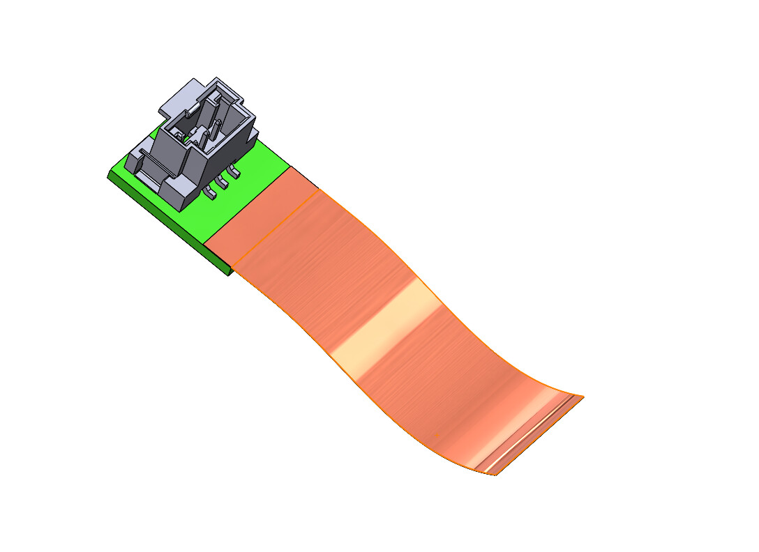
I would start with a double-sided PCB where the bottom side is one electrode and see how small we could get the thing. Do we need a conductive connection to the copper foil or would some capacitive coupling through double-sided tape be feasible somehow? I think I would try to design the gadget like above so that you really could stick it to the surface of the button and provide some contact surface on the top layer of the PCB for manual activation (a conductive connection, i.e., via, to the bottom surface could be enough for that). This contact area could be just a copper fill on the top surface where you could either touch the PCB directly or solder something like a spring, so, effectively flipping the design of the video over.
In case the spring loaded contacts end up being an issue, it might be worthwhile to think of z conductive tape as a backup option (+ maybe it can eliminate the other adhesive tape all together? not sure how strong this one is from personal experience)
The diodes need a constant reverse bias to be totally ‘off’ - but almost zero current is needed in this state, so there needs to be a constant power source.
I thought a bit about the choice of transistor, clearly an NFET, bipolar NPN or even one of those ‘pre-biased’ (with base resistors inside the package) transistors could do the job.
I think it’s a cost decision here- which solution is cheapest? minimizing BOM parts count is key, I think the cost of placing the parts in assembly is on par with the part itself? (for resistors) so eliminating a resistor is a double savings.
The switch will revert to an indeterminate state if you unplug the cable, so floating inputs are not much concern?
With an all-PCB solution, the key idea is minimizing parasitic capacitance between the actual circuit and the electrode, a double-sided board with the parts on one side might suffer a lot of parasitic capacitance, unless you offset the electrode to one side, which is what I was attempting with my prototype.
That could be a good solution, if we made the PCB thin, (1/32”) with a large electrode hanging off one side that you could cut-to-size to adjust for the button you are triggering?
I have found you can cut 1/32” PCB material with just a heavy pair of scissors.
Then you just double-face-tape the unit onto the appliance, right over the button electrode.
I like this- but it’s not clear in my mind how this works practically?
It would be great to eliminate all the extra bits- spring, housing etc.
Maybe it’s possible that this thing could be 100% just a cleverly designed PCB?
I was also thinking about using a flex PCB not just as an electrode, but also for mounting the components to. You would need a stiffener, however. Regarding BOM costs: I think that each component is well below one cent, at least when you select Asian brands and buy full reels. For example, my Asian BSS138 (JSMSEMI) do the job quite well in my other experiments and cost me below 0.005 USD per piece when buying a reel of 3000 pieces. I think that manufacturing costs are more than the components itself. Considering the transistor choice, I think there will be no noticeable price difference (except when we select something exotic), an SOT-23 should have the same assembly costs regardless if it is a BJT or NFET (OK, there might be handling differences with moisture sensitivity levels for baking some sensitive components, but not relevant here, I think).
Your idea of the flex circuit with stiffener is very attractive.
The main electrode could be on the top surface, the substrate is not thick enough to be problematic. This way the board could be single-sided.
The portion with the stiffener would also be attached rigidly with some type of double-sided adhesive tape. The electrode would be flexible to conform to curved surfaces.
You can easily cut the electrode down if it’s too big for a specific application.
I have never done any custom flex circuit designs, there is a lot more to this than the usual simple PCB design process.
The pick-and-place assembly is also complicated by the non-rigid substrate?
It sounds like you might have experience with this subject that you could share with us?
Tooling/extra setup fees?
Assembly and reflow complications?
Can these be arrayed into larger panels for efficiency?
Complications in the design process?
Unfortunately, I had just ordered some prototype flex PCBs from jlcpcb, but never used their assembly service. Neither did I try to order panels, just single PCBs. The order process for flex PCBs (without assembly service) is not that much different from ordering ordinary rigid ones, therefore, I hope someone else can chime in when it comes to flex PCB assembly services. But just looking at the web page at jlcpcb for flex PCB assembly, it does not look cheap.
Thank you, just fixed it. We are scheduling to release the video to the public next week and I didn’t realize that scheduling it would remove it from unlisted status. Thanks!
The flex circuit design represents the super fancy and expensive design.
This 3M tape actually has a conductive adhesive, one could just attach the small PCB with double-face acrylic tape, off to the side, then apply this copper foil tape over the sensor electrode, with a bit overlapping the edge of the PCB, where we have the bare electrode pad.
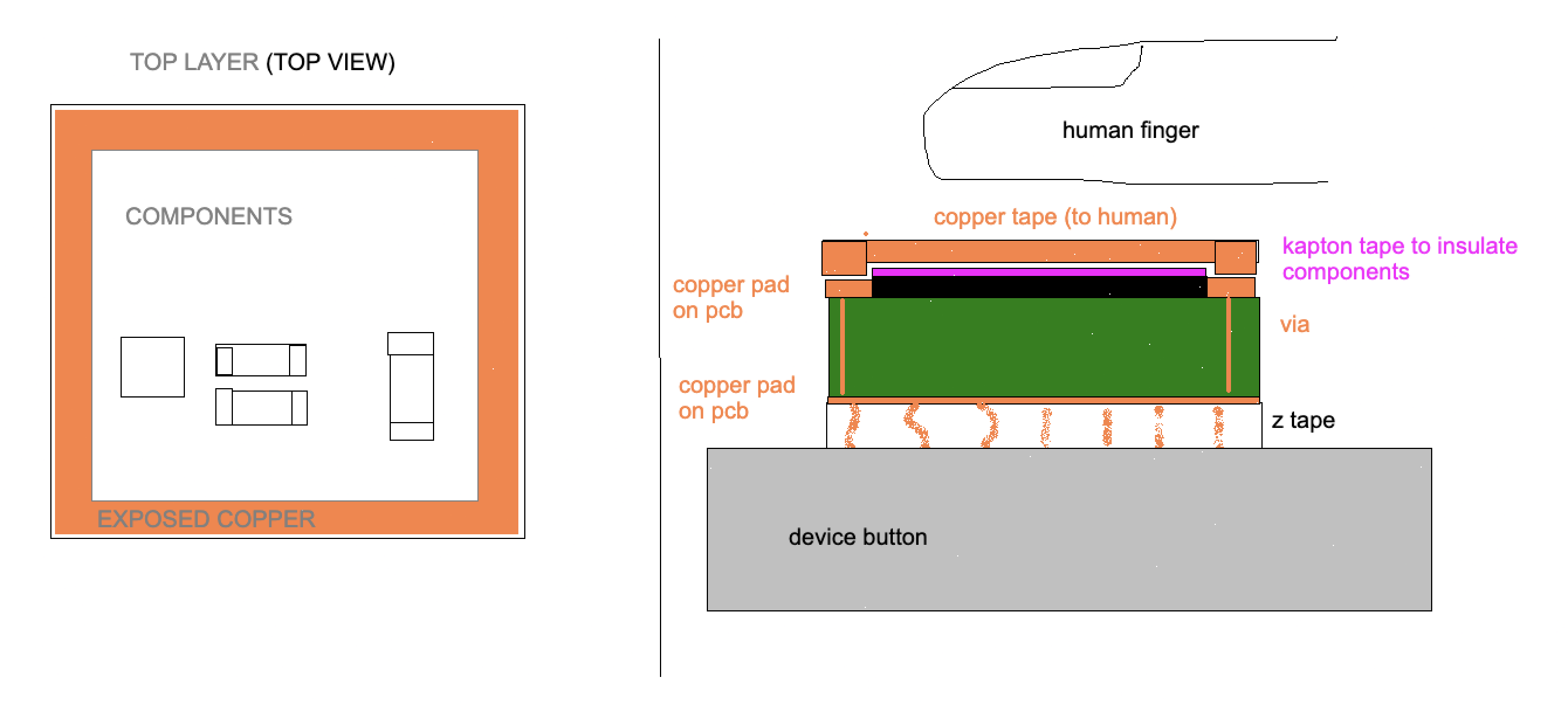
I think so - like what @ksjh suggested I using the z conductive tape at the bottom could offer both mechanical anchoring and electrical connection, as well as the adjustable contact shape that you described in the video (see 3M Z-Axis Conductive Tape 9703 - 2x6 (50mm x 150mm) Strip : ID 1656 : Adafruit Industries, Unique & fun DIY electronics and kits ) and it would also halve the PCB size. The only issue is having the manual activation, but maybe a stackup of z-tape - pcb - kapton tape - copper tape could pass the user’s grounding to the device? The kapton tape would only be there to insulate the pcb components perhaps placed in the middle of the pcb, with a ring of exposed copper connected to the bottom z tape that the top copper tape connects to. A copper tape that is only conductive on one side could be used instead of the one @Leo_Fernekes posted above in which case the kapton tape could be removed.
here’s a little diagram of what i’m talking about (excuse the crude drawing)
That Z-axis tape is really interesting! It’s also fiendishly expensive.
It’s great how this dialogue brings me to learn of new things!
I am trying to think about this project from various points-of-view:
The End User- assumed to be a hobbyist with moderate technical skill, with a low tolerance for expensive monkey business, just wants a cheap and easy solution to a very niche problem. Just peel and stick this device onto the button, plug in a simple cable, give it a test, and off you go. I imagine that it will be important to be able to re-use this thing, or at least re-configure the foil electrode a few times in the process, all without needing to buy another one.
Manufacturing- this is not going to be a huge, high volume thing: there should be very little setup or tooling costs, maybe just a PCB made into a breakaway array for convenience.
I want this to be very easy to say “Yes” to, as a simple thing to add to your module offerings.
A bit of kitting- a little instruction card and some other bits- into a bag with a label.
I think my initial idea of the 3D printed/molded holder is overkill at this point.
We are going to set the Module video live tomorrow, I think that will make things a bit more lively around here!
As I ponder this problem, it occurs to me that maybe I have been overthinking this solution a bit?
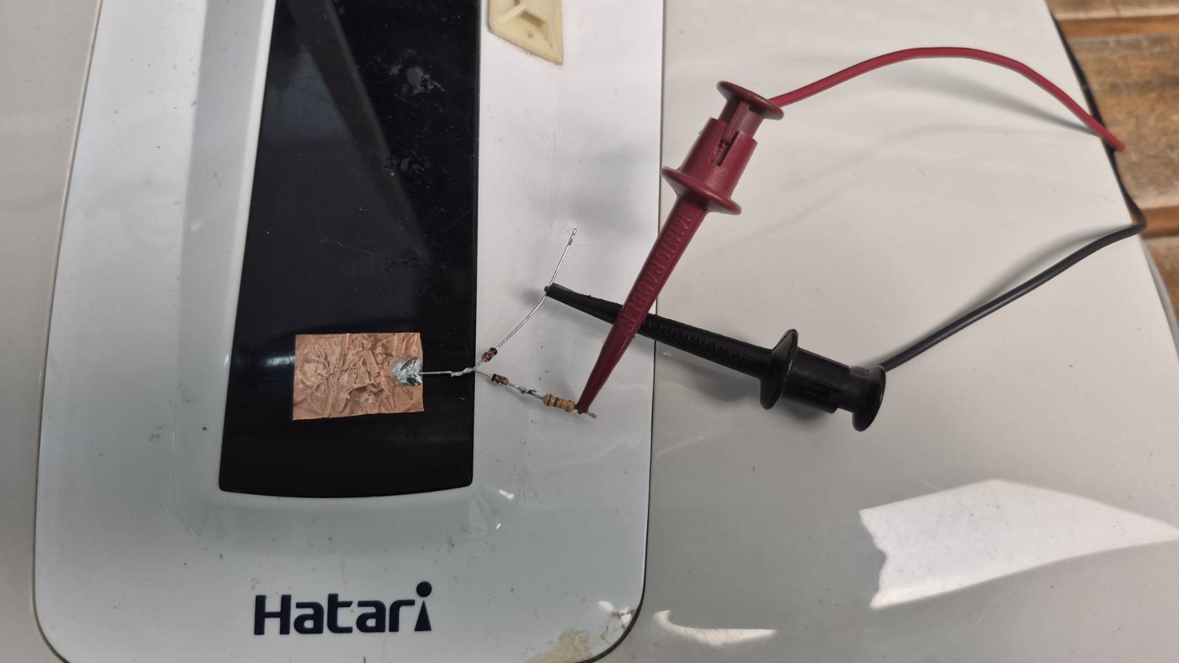
Look at the picture below- I decided to try the dumbest, simplest thing I could think of:
Just 2 x 1N4148 diodes in series with a 10K resistor, and you know what? it totally works!
As long as the voltage on the stimulus electrode never exceeds about 300 mV, or 600 mV P-P, the diodes remain nonconductive, the capacitance is still very low at this point.
3 Volts on the input - and the diodes conduct hard, bringing the electrode to ground, triggering the sensor. I need to test this on more products.