Episode 2: Transistor Inverters, Flip-Flops, and Astable Multivibrators - Full Materials & Discussion
Complete Videos
Part 1
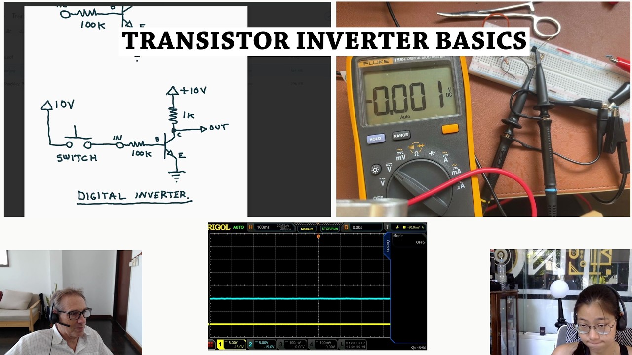
Part 2

Transistors.pdf (4.0 MB)
Learning Objectives
- Understand the internal diode structure of NPN transistors and identify pins using a datasheet and multimeter
- Measure base-emitter reverse breakdown voltage and understand its practical implications
- Build and analyze a transistor inverter circuit, calculating base and collector currents using Ohm’s law
- Explore the difference between linear (active) mode and saturation mode in transistor operation
- Calculate transistor DC current gain (beta) by comparing base current to collector current
- Build a bistable flip-flop by cross-coupling two transistor inverters
- Understand the difference between combinational and sequential logic
- Add LEDs and pushbutton switches to visualize and control flip-flop states
- Convert the bistable circuit into an astable multivibrator using capacitors
- Analyze capacitor coupling and base voltage waveforms on the oscilloscope
- Explore how RC time constants control oscillation frequency
Timestamps
Part 1: Transistor Inverters and Saturation
- 00:00 - Introduction to the bipolar junction transistor (BJT) and the 2N4401 NPN transistor
- 00:27 - The world’s first bipolar transistor invented in 1947 at Bell Labs
- 01:26 - NPN and PNP transistor types as mirror images of each other
- 02:29 - Using the datasheet to identify transistor pins (emitter, base, collector)
- 02:47 - Multimeter diode test to verify internal junctions
- 03:00 - Base-emitter forward bias shows ~0.7V diode drop
- 03:40 - Base-emitter reverse bias shows no conduction
- 04:00 - Base-collector junction also behaves like a diode
- 05:46 - Base-emitter reverse breakdown voltage experiment begins
- 06:23 - Breadboard power supply setup and scope probe configuration
- 08:15 - Breadboard has a break in the middle - adding jumpers
- 09:16 - Observing base-emitter reverse breakdown at ~9 volts
- 12:57 - Building a simple transistor inverter with switch
- 15:00 - Switching demonstration on the oscilloscope
- 16:45 - Adding a pull-down resistor to eliminate noise
- 18:30 - Measuring base voltage and calculating base current (93 microamps)
- 20:00 - Measuring saturation voltage (75mV) and calculating collector current
- 22:00 - Replacing the switch with a 10K potentiometer for variable input
- 24:00 - Observing the three operating regions: cutoff, linear, and saturation
- 26:00 - Calculating transistor gain (beta ≈ 192) in linear mode
- 28:00 - Understanding why saturation requires excess base current
- 32:00 - The concept of saturation as “filling a sponge with water”
- 35:00 - Design criteria for saturated switches in digital circuits
- 42:00 - Final summary of saturated switch operation
Part 2: Flip-Flops and Astable Multivibrators
- 00:00 - Review of the transistor inverter from Part 1
- 00:47 - Building a flip-flop by cross-coupling two inverters
- 02:22 - Resistor color code review (100K = brown, black, yellow)
- 03:00 - Schematic conventions: heavy dots for connections, no dot = crossing
- 04:45 - Grounding both emitters and connecting collector resistors to +10V
- 08:15 - What flip-flops do: fundamental units of digital memory
- 10:57 - Combinational vs sequential logic explained
- 13:40 - Q and Not-Q outputs on the CD4013 flip-flop IC
- 15:00 - Power on and initial state observation on scope
- 16:45 - Troubleshooting channel one scope issue
- 19:30 - Understanding the stable state of the flip-flop
- 20:00 - Manually switching states by grounding the base
- 22:00 - Adding LEDs to visualize current flow
- 26:00 - LED polarity: flat side = cathode, long lead = anode
- 28:00 - Troubleshooting LED issues (blown LEDs from wiring errors)
- 32:00 - Adding 10K resistors across LEDs for proper logic levels
- 36:00 - Pushbutton switches for set and reset functionality
- 41:00 - Creating an astable multivibrator - removing switches
- 45:00 - Converting from bistable to astable by changing resistor connections
- 49:28 - Reducing supply voltage to 7V to avoid base-emitter reverse breakdown
- 50:25 - Adding 10µF capacitors for cross-coupling (plus to collector, minus to base)
- 52:30 - First successful oscillation observed
- 53:45 - Adjusting scope timebase to see the waveform (500ms/div)
- 55:00 - Observing collector and base waveforms simultaneously
- 56:00 - Base voltage going negative (below ground) - the key to operation
- 58:00 - Understanding capacitor charge/discharge through 100K resistors
- 01:00:00 - Why the base goes negative: capacitor as floating voltage source
- 01:03:00 - The role of the 100K resistors: charging path and base current
- 01:07:00 - Experiment: removing the 100K resistors stops oscillation
- 01:09:00 - Which transistor turns on first? Manufacturing variations determine it
- 01:13:00 - Observing the rounded waveform edge from capacitor charging current
- 01:18:00 - Creating asymmetrical timing with different capacitor values (10µF vs 100µF)
- 01:20:00 - Swapping in a 100µF capacitor on one side for longer timing
- 01:23:00 - Observing the dramatic difference in timing between the two sides
- 01:25:00 - Conclusion and encouragement to experiment further
Technical Definitions
Bipolar Junction Transistor (BJT)
A three-terminal semiconductor device with two PN junctions.
Current flows from collector to emitter, controlled by a smaller base current.
Comes in two types: NPN and PNP, which are mirror images of each other.
Base-Emitter Junction
The diode-like PN junction between the base and emitter terminals.
Always forward-biased when the transistor is conducting, with approximately 0.6-0.7V drop.
Acts like a regular silicon diode in terms of voltage drop characteristics.
Reverse Breakdown Voltage
The voltage at which a PN junction begins to conduct in the reverse direction.
For the 2N4401 base-emitter junction, this is approximately 8-9 volts.
Operating beyond this voltage can damage the transistor.
Saturation Mode
The operating state where the transistor is fully turned on.
The collector voltage is pulled as close to ground as possible (typically < 0.1V).
Requires sufficient base current to ensure the transistor cannot conduct more collector current than the circuit allows.
Linear (Active) Mode
The operating state where the transistor is partially conducting.
The collector voltage floats between the supply voltage and ground.
The ratio of collector current to base current equals the transistor’s current gain (beta).
Current Gain (Beta/HFE)
The ratio of collector current to base current in linear mode.
For the 2N4401, typically around 100-300 depending on operating conditions.
Determined experimentally by measuring both currents and calculating the ratio.
Inverter Circuit
A simple digital circuit where a high input produces a low output, and vice versa.
Built with a transistor, base resistor, and collector resistor.
Forms the fundamental building block of digital logic.
Saturated Switch
A transistor circuit designed to be either fully off or fully on.
Requires base current significantly higher than the minimum needed for linear operation.
Ensures clean digital switching with minimal voltage drop in the “on” state.
Bistable Flip-Flop
A sequential logic circuit with two stable states that remembers its state.
Created by cross-coupling two inverters so each output feeds the opposite input.
The most primitive form of digital memory—a single bit storage element.
Combinational Logic
Digital circuits where outputs depend only on current inputs.
Examples include AND, OR, and NOT gates.
Output changes immediately when inputs change.
Sequential Logic
Digital circuits where outputs depend on current inputs AND past states.
Contains memory elements (flip-flops) that retain information.
Examples include counters and state machines.
Set and Reset
Control inputs that force a flip-flop into a specific state.
Set forces the output high (Q = 1); Reset forces the output low (Q = 0).
In the transistor circuit, grounding a base through a switch cuts off that transistor.
Astable Multivibrator
An oscillator circuit with no stable states—continuously switches between two quasi-stable states.
Created by replacing cross-coupled resistors with capacitors in a flip-flop.
The timing is determined by RC time constants (resistor × capacitor values).
Capacitor Coupling
Using capacitors to transfer voltage changes between circuit stages.
When one side of a charged capacitor is pulled to ground, the other side goes negative.
This negative voltage temporarily cuts off the opposite transistor.
Base-Emitter Reverse Breakdown Protection
The base-emitter junction can break down at relatively low reverse voltages (8-9V for 2N4401).
Operating the astable multivibrator at reduced voltage (7V instead of 10V) prevents damage.
Alternative: adding protection diodes to allow higher supply voltages.
RC Time Constant
The product of resistance and capacitance that determines charging/discharging speed.
Larger capacitors or resistors create longer timing periods.
Controls the oscillation frequency in the multivibrator circuit.
Q and Not-Q (Q̄)
Complementary outputs of a flip-flop that are always in opposite states.
When Q is high, Q̄ is low, and vice versa.
In the transistor circuit, the two collector voltages represent Q and Q̄.
Asymmetrical Multivibrator
An astable circuit with different timing on each half-cycle.
Created by using different capacitor values on each side (e.g., 10µF and 100µF).
Produces uneven duty cycles useful for visual effects or specific timing applications.